3-D integrated circuit lateral heat dissipation

a technology of integrated circuits and heat dissipation, which is applied in the field of multitiered (3d) integrated circuits, can solve the problems of increasing thermal density, hot spots, and little ability to move heat away from heat sources, and achieves the effect of assisting heat dissipation

Active Publication Date: 2013-08-06
QUALCOMM INC
View PDF35 Cites 2 Cited by
  • Summary
  • Abstract
  • Description
  • Claims
  • Application Information

AI Technical Summary

Benefits of technology

[0009]Embodiments of the invention fill an air gap between stacked dies with a thermally conductive material, which allows heat generated at one or more locations within each die to be laterally displaced. The lateral displacement of the heat can be along the full length of the die or along a portion of the length. In one embodiment, the thermal material is electrically insulating. In one embodiment, TSVs, perhaps using carbon nanotubes can be constructed at certain locations to assist in heat dissipation away from thermally troubled locations.

Problems solved by technology

One problem when dies are positioned in close proximity to each other is that thermal density increases.
Thus, hot spots could exist with little ability to move the heat away from the heat source.
Another method is to increase the metal layers in the chip to be able to dissipate heat This, in turn, negatively impacts the desired aspect ratio of the package, as well as degrades the signal transmission speeds.
An additional problem exists when more than one tier is bonded.
Oxide, being a poor thermal conductor, adds to the heat dissipation problem.
A problem with such a solution is that a circuit layout may prevent positioning a TSV at the necessary location because of devices constructed in the various tiers in proximity to the hot spot generating the heat.
This is costly to manufacture because the moving liquid requires a pumping mechanism and tight tolerances for liquid channels.
Also, it may not be possible to channel the cooling material to the necessary location.
The channeling problem could be overcome, to some extent, by forcing cooling liquid through the substrate itself, but this method is not without a further set of problems and costs.

Method used


Image

  • 3-D integrated circuit lateral heat dissipation
  • 3-D integrated circuit lateral heat dissipation
  • 3-D integrated circuit lateral heat dissipation

Examples


Embodiment Construction

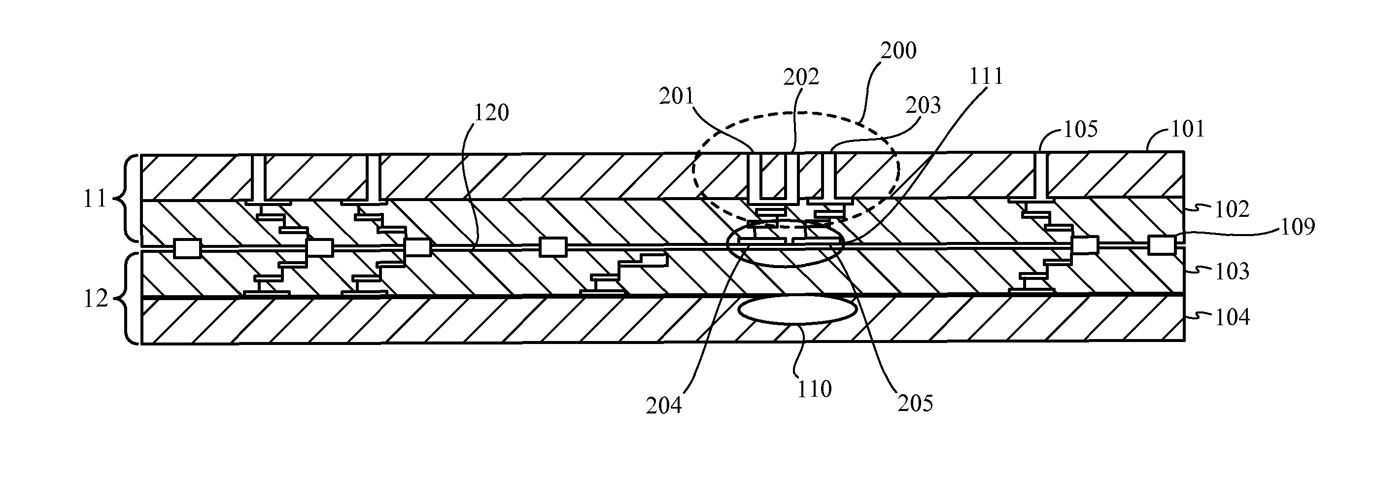
[0019]FIG. 1 illustrates one aspect of thermal trouble conditions that could exist with 3-D integrated circuits. As shown in FIG. 1, a die 11 is stacked with a die 12. The active layer of die 11 is a layer 102 and the active layer of die 12 is a layer 103. This is an exemplary arrangement as the active layers of the dies could be in any orientation, up or down.

[0020]Vias 105 run through the substrate layer 101 of the die 11. Vias could be constructed in the layers 102, 103 and / or 104 as desired. Electrical paths 107 and 108 form an interconnect between the dies. Seal 109 acts to prevent non-desired contaminants from entering the area 120 between the respective dies 11, 12.

[0021]Element 108 is normally on the scale of 30 microns or less and normally forms a copper or a tin copper metal to metal bond. Area 120 is usually an air gap. The gap 120 can be in the range of less than 10 micron.

[0022]A hot spot 110 is on the die 12 and the challenge is to move heat from this relatively small ...


PUM


Abstract

By filling an air gap between tiers of a stacked IC device with a thermally conductive material, heat generated at one or more locations within one of the tiers can be laterally displaced. The lateral displacement of the heat can be along the full length of the tier and the thermal material can be electrically insulating. Through silicon-vias (TSVs) can be constructed at certain locations to assist in heat dissipation away from thermally troubled locations.

Description

FIELD OF DISCLOSURE[0001]This disclosure relates to integrated circuits (ICs), and more specifically to multi-tiered (3-D) ICs, and even more specifically to systems and methods for enhancing heat dissipation in 3-D ICs.BACKGROUND[0002]In IC technology there is a need to stack the chips (dies) together to form multi-tiered or three-dimensional (3-D) IC devices. One result of such 3-D IC stacking is a decrease of signal propagation time during signal processing, due to the reduced distance signals must travel when they remain within a single package.[0003]One method for tier bonding is to bring two (or more) dies together and then encapsulate the dies into a single structure. Electrical conductors and / or contacts on the surface of the respective dies serve to carry electrical signals between components on the different dies.[0004]One problem when dies are positioned in close proximity to each other is that thermal density increases. Moreover, because of the reduced size of stacked IC...

Claims


Application Information

Patent Timeline
Patent Type & Authority Patents(United States)
IPC IPC(8): H01L23/34
CPCH01L23/3677H01L23/3732H01L23/3735H01L25/0657H01L2924/01019H01L2224/16145H01L2225/06513H01L2225/06589
Inventor KASKOUN, KENNETHGU, SHIQUNNOWAK, MATTHEW
Owner QUALCOMM INC
Why Eureka
Try Eureka