Spread spectrum clock generation circuit and a method of controlling thereof

a technology of a spread spectrum clock and a control method, which is applied in the direction of pulse automatic control, angle demodulation by phase difference detection, electrical equipment, etc., can solve the problems of increasing circuit scale, increasing undesirable jitter, and power saving cannot be expected, so as to reduce electromagnetic interference emission, reduce current consumption, and reduce jitter

Active Publication Date: 2013-08-06
CYPRESS SEMICON CORP
View PDF18 Cites 6 Cited by
  • Summary
  • Abstract
  • Description
  • Claims
  • Application Information

AI Technical Summary

Benefits of technology

[0017]The invention is directed to overcoming at least one of the problems described in “Background of the Invention”, and a primary object of the invention is therefore to provide a spread spectrum clock generation circuit and a method of controlling a spread spectrum clock generation circuit, which ensure clock generation accompanied with less jitter and ideal spread spectrum and enable use of a small-scale circuit and, in consequence, lower power consumption.
[0023]With the above arrangement, the invention provides the following effects. First of all, according to the invention, the control of the voltage (hereinafter referred to as “modulation voltage”) for modulating the frequency of the output signal of the voltage control oscillator circuit is carried out by controlling a charge / discharge current for the capacitor unit. More specifically, the capacitor unit is charged or discharged and outputs a modulation voltage obtained by current-voltage conversion. Since the voltage level of the modulation voltage output from the capacitor unit continuously varies in accordance with the amount of charge in the capacitor unit, the voltage level smoothly changes without causing abrupt discontinuous changes at the points of switching between a charge phase and a discharge phase. As a result, clocks accompanied with less jitter and ideal spread spectrum become possible, which highly contributes to a reduction in electromagnetic interference emission.
[0024]Secondly, in the invention, the control of the signal for modulating the frequency of the output signal is performed with current, whereas a voltage control oscillator circuit is used as the oscillator circuit. In this arrangement, current-voltage conversion is carried out in the capacitor unit. Thus, the use of the voltage control oscillator circuit reduces current consumption, compared to cases where a current control oscillator is used, so that power saving can be achieved.
[0025]Thirdly, the invention is designed to switch the current path with the switching unit. This makes it possible to employ circuit configuration simpler than the conventional complicated circuit configurations which involve a divider, up-down counter, divider counter, switching circuit and others. The circuit according to the invention employs a less number of capacitors, thereby reducing circuit space occupied by the capacitors which generally require a large space, in contrast with the prior cases employing a plurality of capacitors. This enables a reduction in circuit scale. In addition, use of a small-scale circuit leads to power saving.

Problems solved by technology

At that time, the frequency of the output signal CK excessively varies before and after the switching of the capacitor, which sometimes increases undesirable jitter.
This disadvantageously causes an increase in circuit scale.
Since this control is current control, power is consumed at all times in the current digital-analog converter 243 and therefore power saving cannot be expected.

Method used


Image

  • Spread spectrum clock generation circuit and a method of controlling thereof
  • Spread spectrum clock generation circuit and a method of controlling thereof
  • Spread spectrum clock generation circuit and a method of controlling thereof

Examples


first embodiment

[0042]Referring now to the accompanying drawings and, more particularly, to FIGS. 1 to 9, a spread spectrum clock generation circuit and a method of controlling a spread spectrum clock generation circuit will be hereinafter described in detail according to preferred embodiments. the invention will be described with reference to FIGS. 1 to 4.

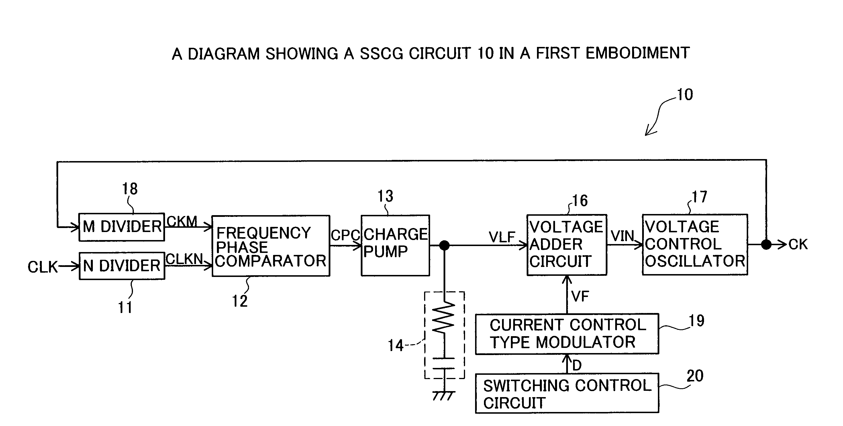
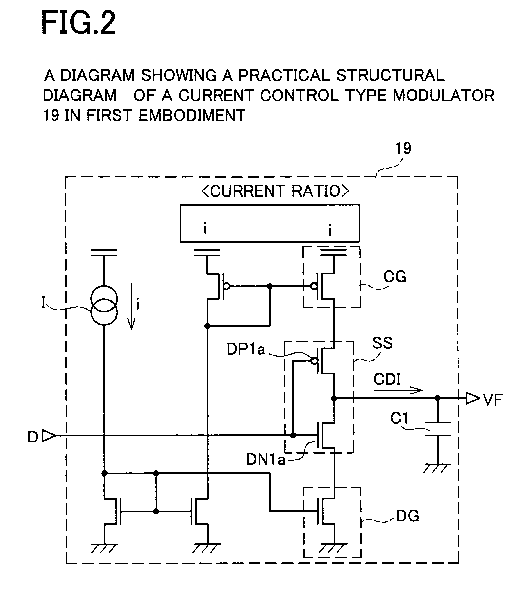
[0043]FIG. 1 shows an SSCG circuit 10 which is constructed based on a PLL circuit configuration. The SSCG circuit 10 includes an N divider 11, a frequency phase comparator 12, a charge pump 13, a loop filter 14, a voltage adder circuit 16, a voltage control oscillator 17, an M divider 18, a current control type modulator 19 and a switching control circuit 20.

[0044]The N divider 11 outputs a signal CLKN obtained by dividing a basic clock signal CLK. The M divider 18 outputs a signal CKM obtained by dividing an output signal CK. The frequency phase comparator 12 detects the phase difference between the signals CLKN and CKM to output a control signa...

second embodiment

[0074]As fully discussed in the above description, the SSCG circuit of the second embodiment is formed such that by changing charge / discharge current according to the modulation cycles, the charge / discharge amounts for all the modulation cycles can be made equal. Therefore, the fluctuation range of the frequency of the output signal from the voltage control oscillator becomes constant in all of the modulation cycles. This makes the lengths of holding time for the oscillation frequencies within the fluctuation range even. Since the spectrum waveform after the spread spectrum modulation has a flat peak profile, the maximum value of spectrum intensity can be made smaller. In consequence, electromagnetic interference emission can be reduced and, therefore, malfunctions or the like due to the mutual interference between electronic devices can be prevented without fail.

[0075]It is apparent from the above discussion that the invention is not necessarily limited to the particular embodiment...


PUM


Abstract

A spread spectrum clock generation circuit and a controlling method thereof are disclosed, which provide clocks having less jitter and ideal spread spectrum and enable a reduction in circuit scale and in power consumption. To this end, a current control type modulator 19a is equipped with a current source Ia (current 4i). A charger unit CGa and a discharger unit DGa are designed such that currents i, 2i and 4i are allowed to flow, for example, by properly setting the sizes of transistors. Modulation cycles CIa to CIIIa are repeated and an output code is generated from a switching control circuit 20a according to each modulation cycle. A switching unit SSa is controlled according to the output code, thereby charging or discharging a capacitor element C1 with a charge / discharge current CDI corresponding to the output code. Hence, charge amounts and discharge amounts for all the modulation cycles CIa to CIIIa have the same value, i.e., 6i [A·clock].

Description

CROSS-REFERENCE TO RELATED APPLICATIONS[0001]This application is based upon and claims the benefit of priority from each of the prior Japanese Patent Application No. 2005-030917 filed on Feb. 7, 2005, the entire contents of which are incorporated herein by reference.BACKGROUND OF THE INVENTION[0002]1. Field of the Invention[0003]The present invention relates to a spread spectrum clock generation circuit which generates clock signals having a minutely varying cycle to reduce electromagnetic interference emission and a method of controlling the spread spectrum clock generation circuit.[0004]2. Description of Related Art[0005]FIG. 9 shows the configuration of the spread spectrum clock generation circuit (hereinafter referred to as “SSCG circuit”) 200 disclosed in Japanese Unexamined Patent Publication No. 2004-207846. An analog modulator 119 generates a modulation signal VF according to control performed by a switching control circuit 120. The modulation signal VF is added to a control...

Claims


Application Information

Patent Timeline
Patent Type & Authority Patents(United States)
IPC IPC(8): H04B1/69H03L7/093H03L7/18H04B1/707
CPCH03L7/08H04B1/707H03L7/18
Inventor SAITO, SYUICHIOKADA, KOJI
Owner CYPRESS SEMICON CORP
Why Eureka
Try Eureka