Method for manufacturing an electronic assembly

a manufacturing method and electronic assembly technology, applied in the direction of printed circuit manufacturing, printed circuit aspects, printed electric component incorporation, etc., can solve the problems of difficult to precisely position electronic components and comparatively large thickness, and achieve cost-effective wiring and encapsulation. , the effect of cost-effectiv

Active Publication Date: 2013-08-13
ROBERT BOSCH GMBH
View PDF16 Cites 2 Cited by
  • Summary
  • Abstract
  • Description
  • Claims
  • Application Information

AI Technical Summary

Benefits of technology

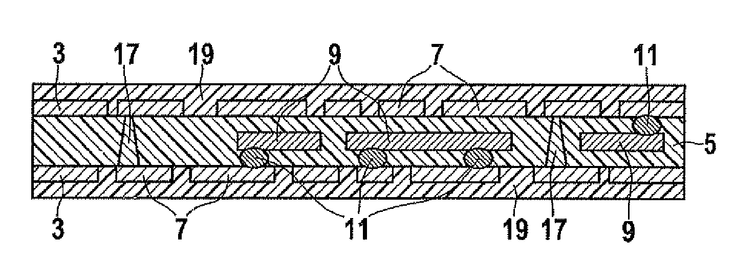
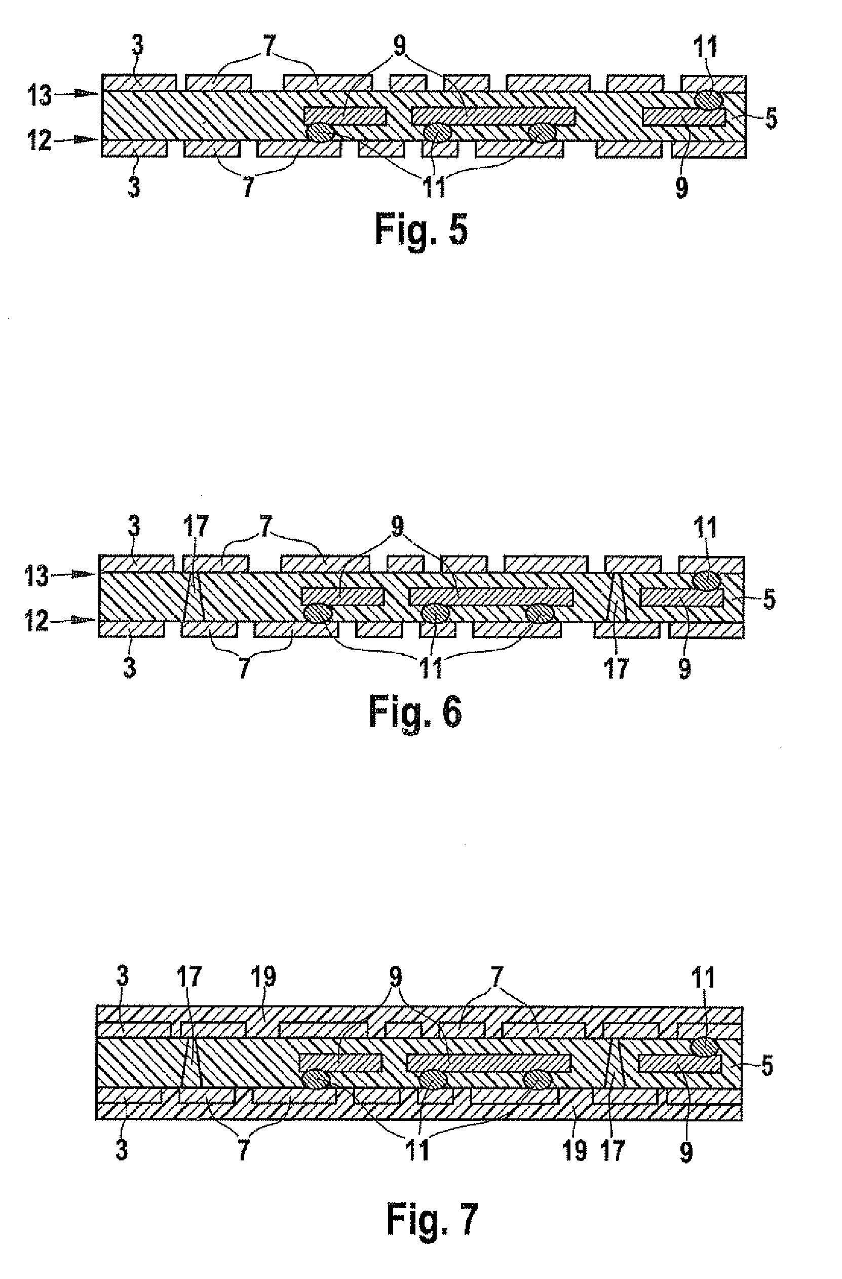
[0010]By laminating the foil onto the conductive foil equipped with the at least one electronic component on the side on which the conductive foil is equipped with the at least one electronic component, the component is completely encapsulated. A high reliability, in particular of sensitive components, is thereby achieved.
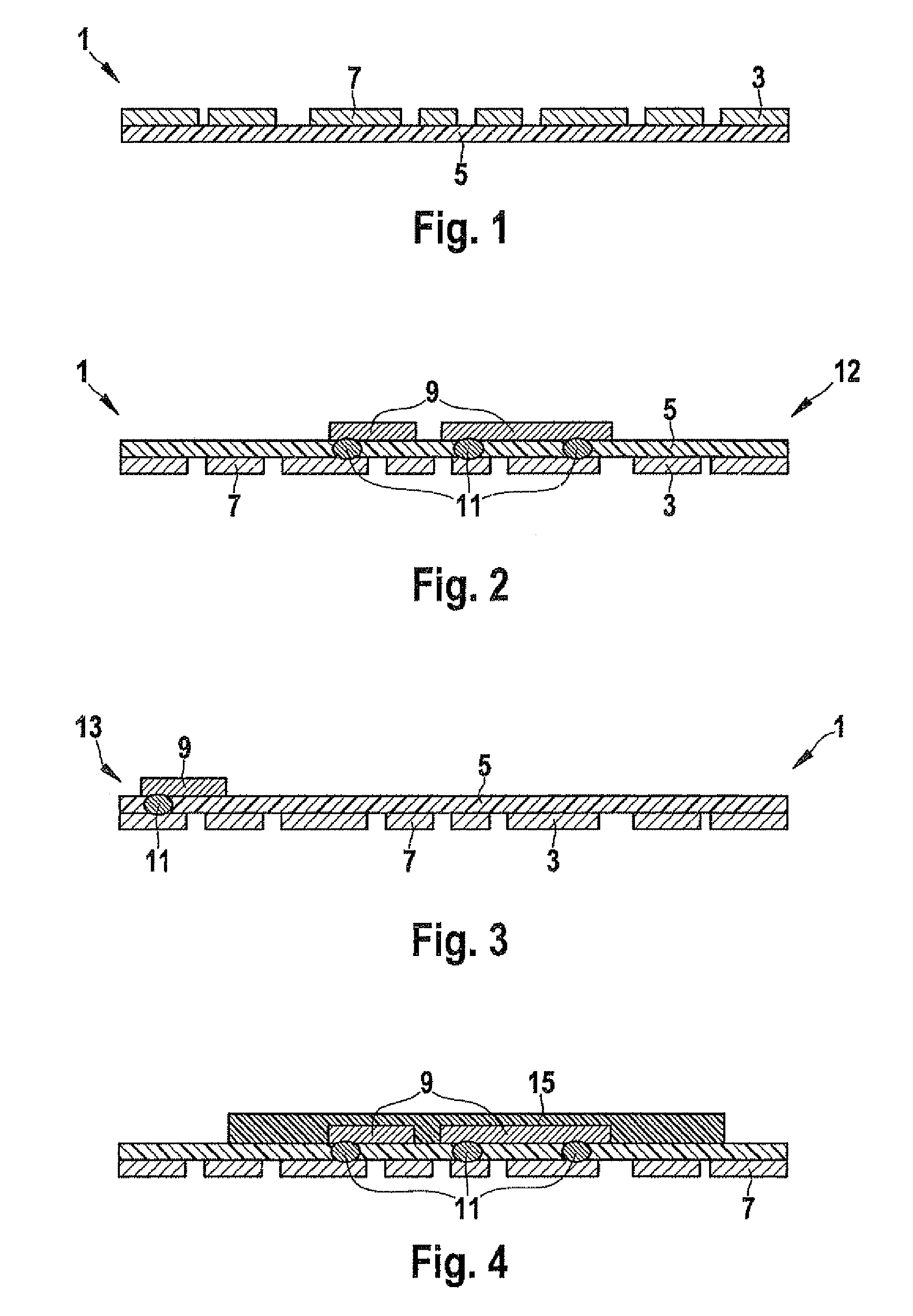
[0012]In one specific embodiment, the additional foil, which is laminated on the conductive foil equipped with the at least one electronic component, is also a conductive foil, which is equipped with at least one electronic component. The lamination may occur in such a way that the electronic components of the two foils face each other such that the conductive foils are located on the outside of the laminate. In this manner, the surface area utilization may be increased markedly. In order to prevent the lamination of the additional foil on the conductive foil from producing undesired electrical connections, a layer made of a dielectric material may be inserted between the two conductive foils. The layer inserted between the two conductive foils may be a plastic layer. A thermoplastic is used as the plastic for example. It is also possible, however, to use any other plastic. The layer that is introduced between the two conductive foils may be used to fix the components in place and to ensure the contacting.
[0013]In order to insert the plastic layer between the two conductive foils, it is possible for example to apply a plastic coating on the conductive foil prior to equipping it with the at least one electronic component. The plastic coating may be applied prior to or after patterning the foil to form the circuit trace structure. The application of the plastic coating prior to patterning the conductive foil has the advantage that, because of the plastic layer, a continuous base is preserved, on which the metal layer is patterned. As a result, individual circuit traces will not be shifted or bent for example by careless handling. By contrast, if the conductive foil is not provided with a plastic layer, it is necessary to leave the conductive foil on a carrier, it then being necessary to handle the patterned foil so carefully that individual circuit traces of the structure do not shift or bend.
[0016]In order to prevent undesired contacts on the conductive foil, which result in a malfunction of the electronic assembly for example, an insulating layer may be applied on at least one of the outward facing sides of the electronic assembly. In insulating layer is usually made of a dielectric material. Plastics are especially suitable as insulating layers. Particularly if the electronic assembly is to be deformed, it is advantageous if the insulating layer is made from a thermoplastic material.
[0024]Using the method according to the present invention it is possible to achieve a cost-effective wiring and encapsulation by using processes on many modules simultaneously and a reel-to-reel manufacture. It is moreover possible to process the electronic assembly further as a standard component for example. In the method according to the present invention, the electronic components are contacted during assembly. This requires fewer process steps than in the methods known from the related art.

Problems solved by technology

A disadvantage of this assembly is that initially receptacles are cut into the circuit board substrate, into which the electronic components inserted.
This makes it very difficult to position the electronic components precisely.
Additional disadvantages of the electronic assemblies known from the related art are their comparatively great thickness due to the circuit board substrate used.
Furthermore, the electronic assemblies manufactured according to the related art are rigid and not deformable.

Method used


Image

  • Method for manufacturing an electronic assembly
  • Method for manufacturing an electronic assembly
  • Method for manufacturing an electronic assembly

Examples


Embodiment Construction

[0036]FIGS. 1 through 7 show individual method steps for manufacturing an electronic component developed in accordance with the exemplary embodiments and / or exemplary methods of the present invention.

[0037]In a first step, which is shown in FIG. 1, an electrically conductive foil 1 is patterned so as to develop a circuit trace structure. The patterning is performed only on an electrically conductive layer 3 of electrically conductive foil 1. In the specific embodiment shown here, electrically conductive layer 3 is applied on an electrically non-conductive layer 5. Electrically non-conductive layer 5 acts as a carrier layer and is not patterned. Electrically non-conductive layer 5 is a plastic layer for example. Particularly metals, for example copper or silver, are suitable as electrically conductive layer 3. Furthermore, gold, palladium or laminates, for example NiPdAu, are suitable as well. Electrically non-conductive layer 5 may be applied on electrically conductive layer 3 by la...


PUM

PropertyMeasurementUnit
electrically conductiveaaaaaaaaaa
electricallyaaaaaaaaaa
conductiveaaaaaaaaaa

Abstract

A method for manufacturing an electronic assembly, including at least one electronic component and a circuit trace structure, by which the at least one electronic component is contacted. In the method, a conductive foil is patterned in a first step to form the circuit trace structure. In a second operation, the circuit trace structure is equipped with the at least one electronic component. In a final operation, another foil is laminated onto the conductive foil equipped with the at least one electronic component on the side on which the conductive foil is equipped with the at least one electronic component.

Description

FIELD OF THE INVENTION[0001]The present invention relates to a method for manufacturing an electronic assembly, including at least one electronic component and a circuit trace structure, by which the at least one electronic component is contacted.BACKGROUND INFORMATION[0002]Electronic components used for manufacturing the electronic assembly are integrated circuits (IC) for example. These are accommodated in a substrate, for example in order to encapsulate them and to increase the surface area utilization on the electronic circuit carrier. This makes it possible to protect the electronic components. U.S. Pat. No. 6,512,182, for example, discusses cutting receptacles into a circuit board substrate, into which the electronic components are inserted. Once the electronic components have been inserted, the receptacles are filled, then smoothed and laminated over. Embedding the electronic components makes it possible to achieve a smooth surface of the electronic assembly.[0003]A disadvant...

Claims


Application Information

Patent Timeline
Patent Type & Authority Patents(United States)
IPC IPC(8): H05K3/30
CPCH01L21/4825H01L23/5389H01L24/18H01L24/82H05K1/186H01L23/5387Y10T29/49126H01L2221/68377H01L2224/16237H01L2224/18H01L2924/01029H01L2924/01033H01L2924/01046H01L2924/01047H01L2924/01079H01L2924/01082H01L2924/14H05K1/0284H05K1/189H05K3/0014H05K3/4038H05K2201/0305H05K2201/0355H05K2201/10674H05K2203/302H01L2924/01005H01L2924/01006H01L2924/01068H01L2924/014H01L2924/07802Y10T29/49165Y10T29/4913H01L2924/00H01L2924/181H01L2224/05573H01L2224/05568H01L2924/00014H01L24/96H01L2224/05599
Inventor SCHAAF, ULRICHKUGLER, ANDREAS
Owner ROBERT BOSCH GMBH
Why Eureka
Try Eureka