Light emitting diode package

a technology of light-emitting diodes and packages, which is applied in the direction of electrical equipment, semiconductor devices, instruments, etc., can solve the problems of enlarging the size of backlight modules, and achieve the effect of improving the uniformity of white light l′ and high directivity

Active Publication Date: 2013-08-13
CORETRONIC
View PDF13 Cites 7 Cited by
  • Summary
  • Abstract
  • Description
  • Claims
  • Application Information

AI Technical Summary

Benefits of technology

[0010]Accordingly, the invention is to provide a light emitting diode package for achieving uniform mixing light.
[0011]One embodiment of the invention provides a light emitting diode package includes a substrate, a plurality of light emitting diode chips, a fluorescence layer, and a plurality of reflecting layers. The light emitting diode chips, the fluorescence layer, and the reflecting layers are disposed on the substrate. The fluorescence layer covers the light emitting diode chips, and the reflecting layers are disposed above the fluorescence layer and right above the light emitting diode chips, respectively. The reflecting layers are disposed on a same level, and each of the reflecting layers is a diffusion reflecting layer with high reflectivity, high diffusivity and low transmittance.
[0018]Compared to the conventional, each of the reflecting layer is capable of reflecting the light beam back to the fluorescence layer in the invention, so that the light beam with high directivity is emitted out between two adjacent light emitting diode chips after back and forth movement in the fluorescence layer so as to improve uniformity of the white light L′ emitted from the light emitting diode package and solves the problem of big size of the lengthened or thickened light guide plate when the light emitting diodes are disposed in the light guide plate of the conventional backlight module.

Problems solved by technology

Thus, how to improve the light mixing efficiency of the backlight module and also avoid enlarging the size of the backlight module are urgent problems in the art.

Method used


Image

  • Light emitting diode package
  • Light emitting diode package
  • Light emitting diode package

Examples


Embodiment Construction

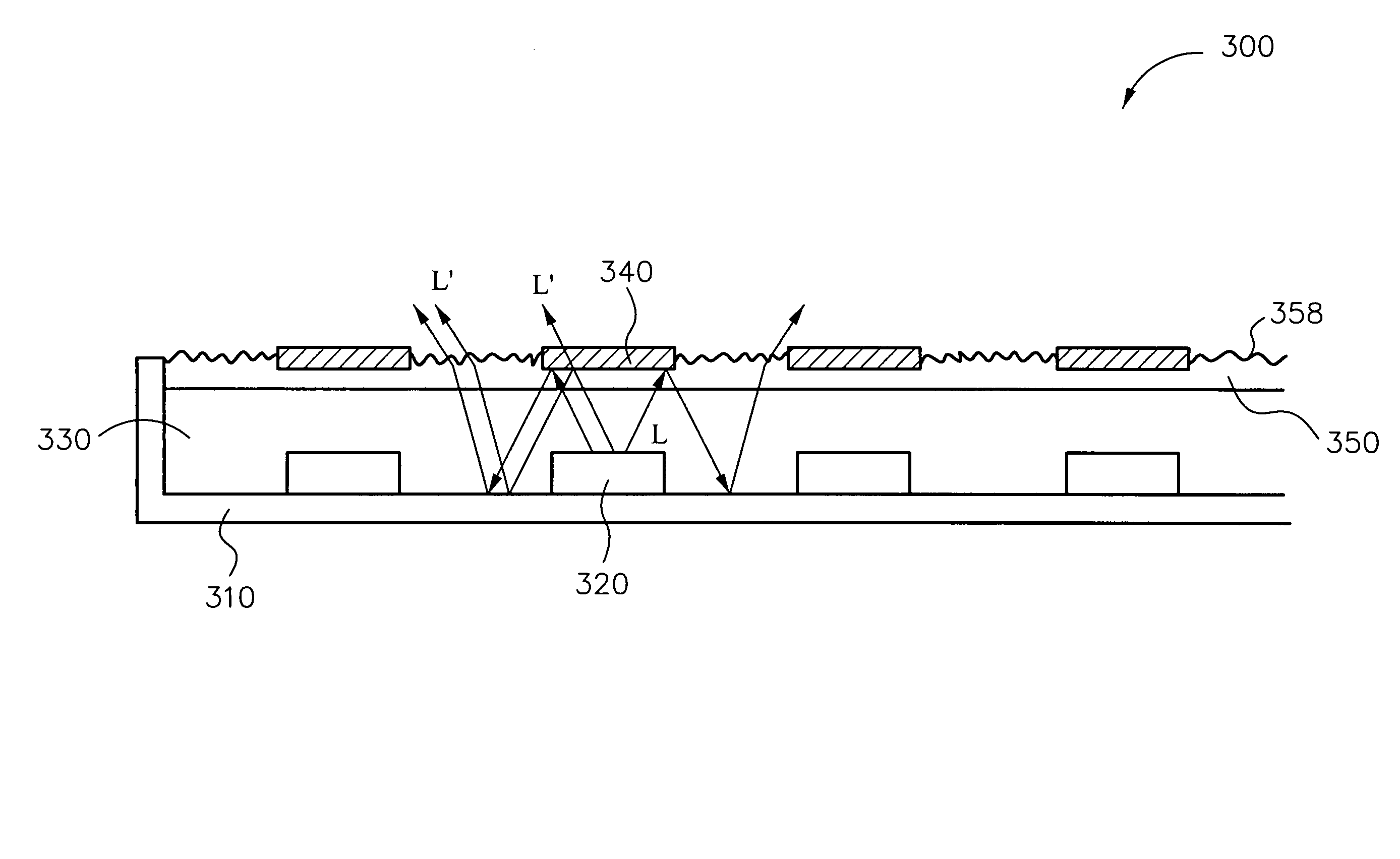
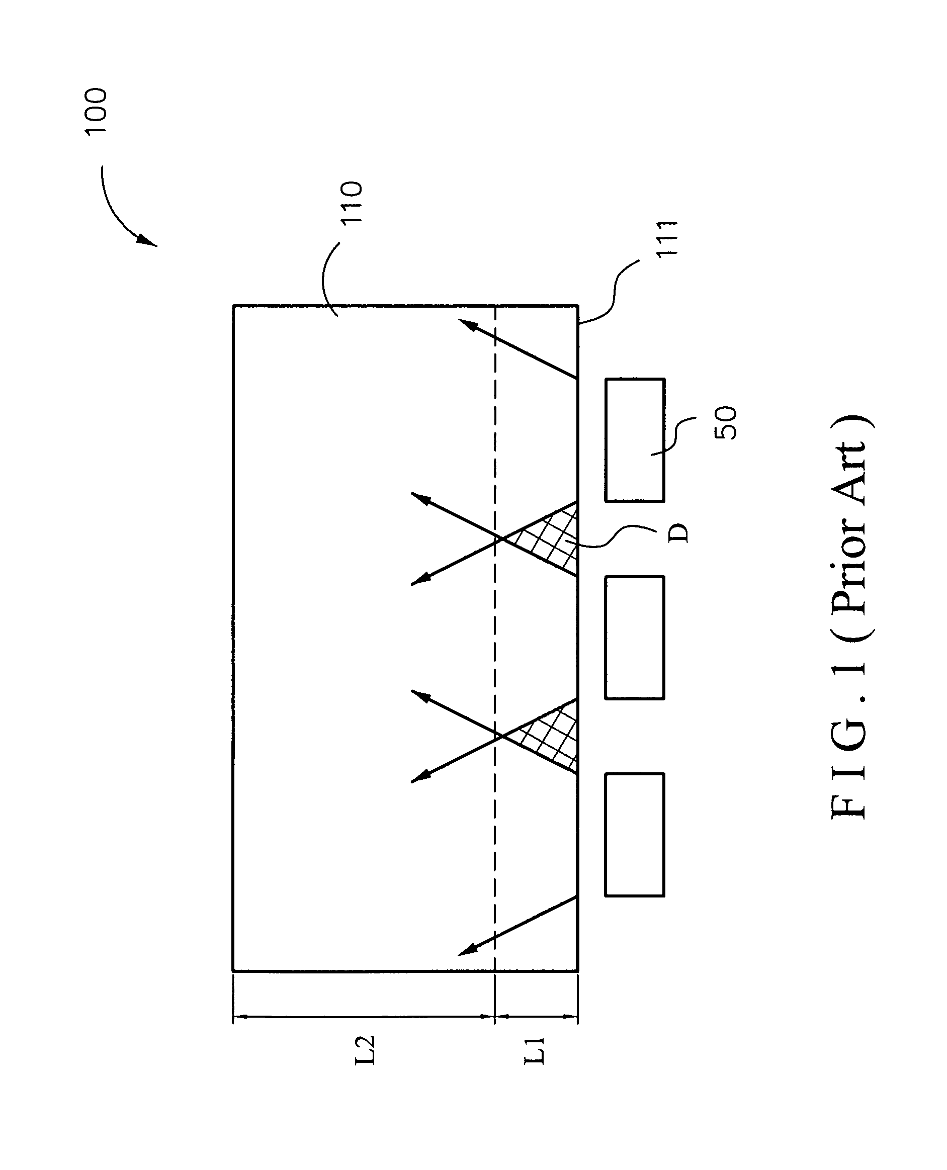
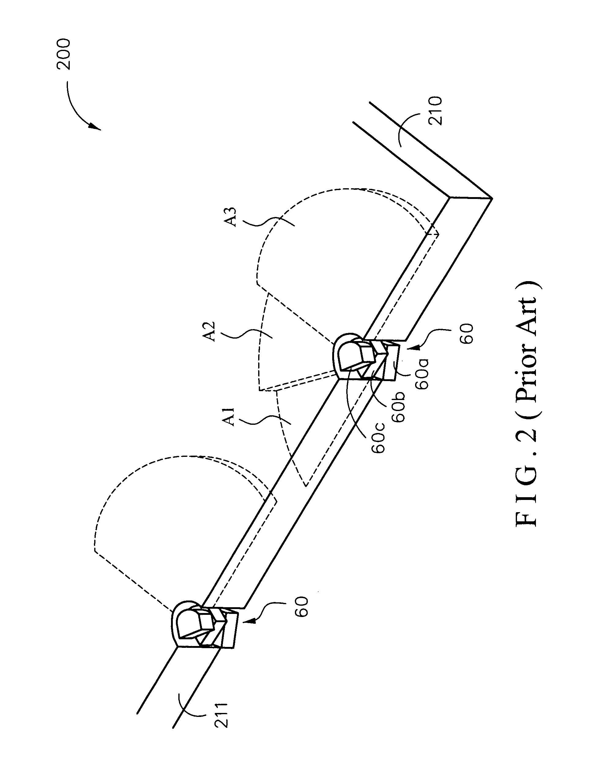
[0027]In the following detailed description of the preferred embodiments, reference is made to the accompanying drawings which form a part hereof, and in which are shown by way of illustration specific embodiments in which the invention may be practiced. In this regard, directional terminology, such as “top,”“bottom,”“front,”“back,” etc., is used with reference to the orientation of the Figure(s) being described. The components of the present invention can be positioned in a number of different orientations. As such, the directional terminology is used for purposes of illustration and is in no way limiting. On the other hand, the drawings are only schematic and the sizes of components may be exaggerated for clarity. It is to be understood that other embodiments may be utilized and structural changes may be made without departing from the scope of the present invention. Also, it is to be understood that the phraseology and terminology used herein are for the purpose of description an...


PUM


Abstract

A light emitting diode package includes a substrate, a plurality of light emitting diode chips, a fluorescence layer, and a plurality of reflecting layers. The light emitting diode chips, the fluorescence layer, and the reflecting layers are disposed on the substrate. The fluorescence layer covers the light emitting diode chips, and the reflecting layers are disposed right above the light emitting diode chips, respectively.

Description

BACKGROUND OF THE INVENTION[0001](1) Field of the Invention[0002]The invention relates to a light emitting diode package, and more particularly to a light emitting diode package of a backlight module.[0003](2) Description of the Related Art[0004]light emitting diode (LED) is a kind of semiconductor component, and is popularized as light source of a backlight module in a display due to small size, long life, low driving voltage, quick response, good seismic resistance, and ability to meet requirements of lightness, thinness and miniaturization of various devices. Light source of the backlight module in the display of common information products is always white light, so that the light emitting diode needs to generate uniform white light. In the current backlight module, white light is generated by mixing light generated from the light emitting diodes at entrance of the light guide plate.[0005]Refer to FIG. 1 for a profile view of a conventional light emitting diode package 50 applied...

Claims


Application Information

Patent Timeline
Patent Type & Authority Patents(United States)
IPC IPC(8): H01L21/18H01L33/00
CPCG02F1/133603G02F1/133605G02F1/133606G02F2001/133614G02F1/133614
Inventor WENG, CHAO-HUNGCHUANG, FU-MING
Owner CORETRONIC
Why Eureka
Try Eureka