
Cascaded cure approach to fabricate highly tensile silicon nitride films

a silicon nitride film, highly tensile technology, applied in the field of high tensile dielectric films, can solve problems such as significant stress changes, and achieve the effect of reducing shrinkage and film relaxation and reducing the stress

Inactive Publication Date: 2013-08-20
NOVELLUS SYSTEMS
View PDF301 Cites 21 Cited by
  • Summary
  • Abstract
  • Description
  • Claims
  • Application Information

AI Technical Summary

Benefits of technology

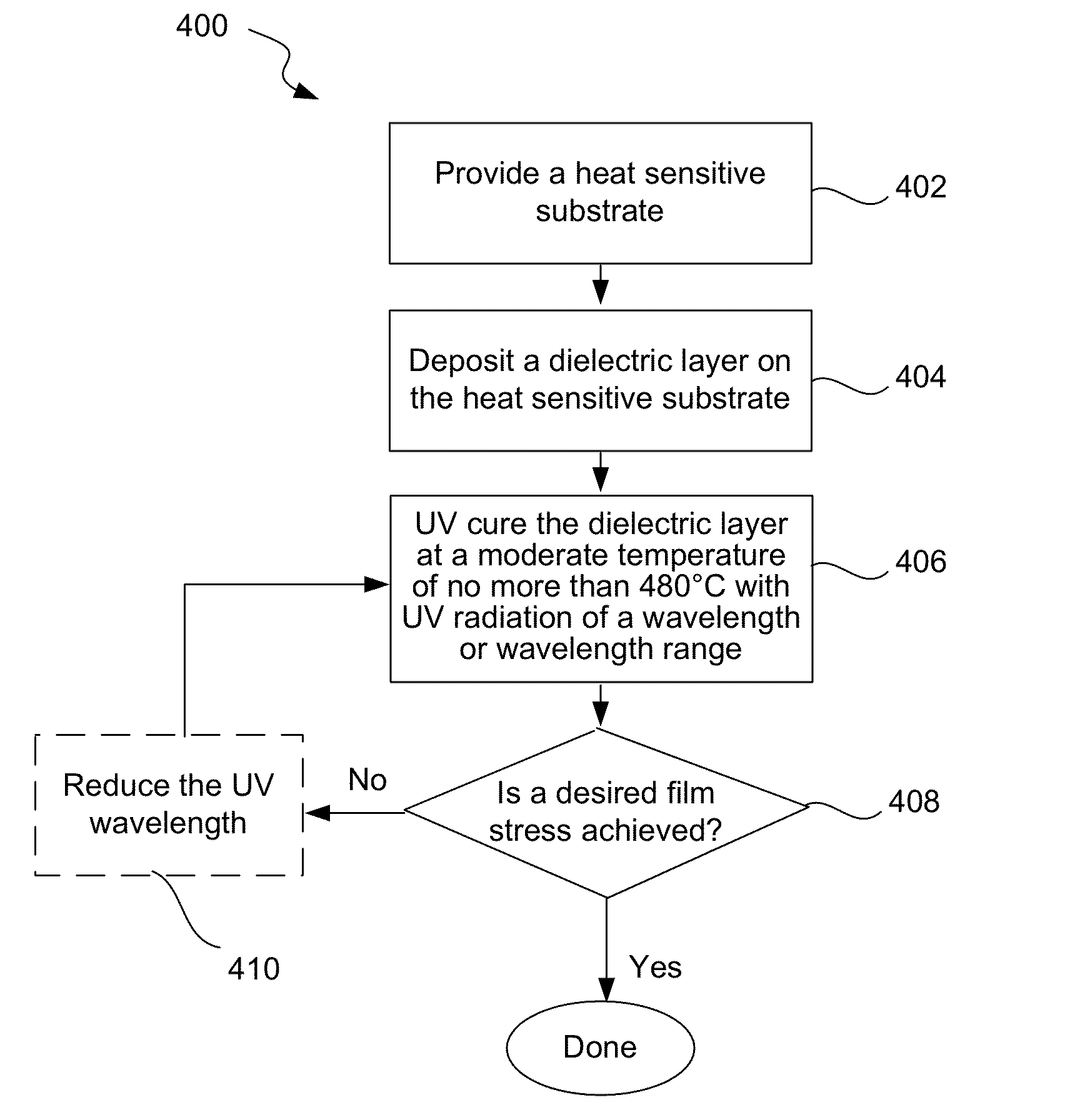
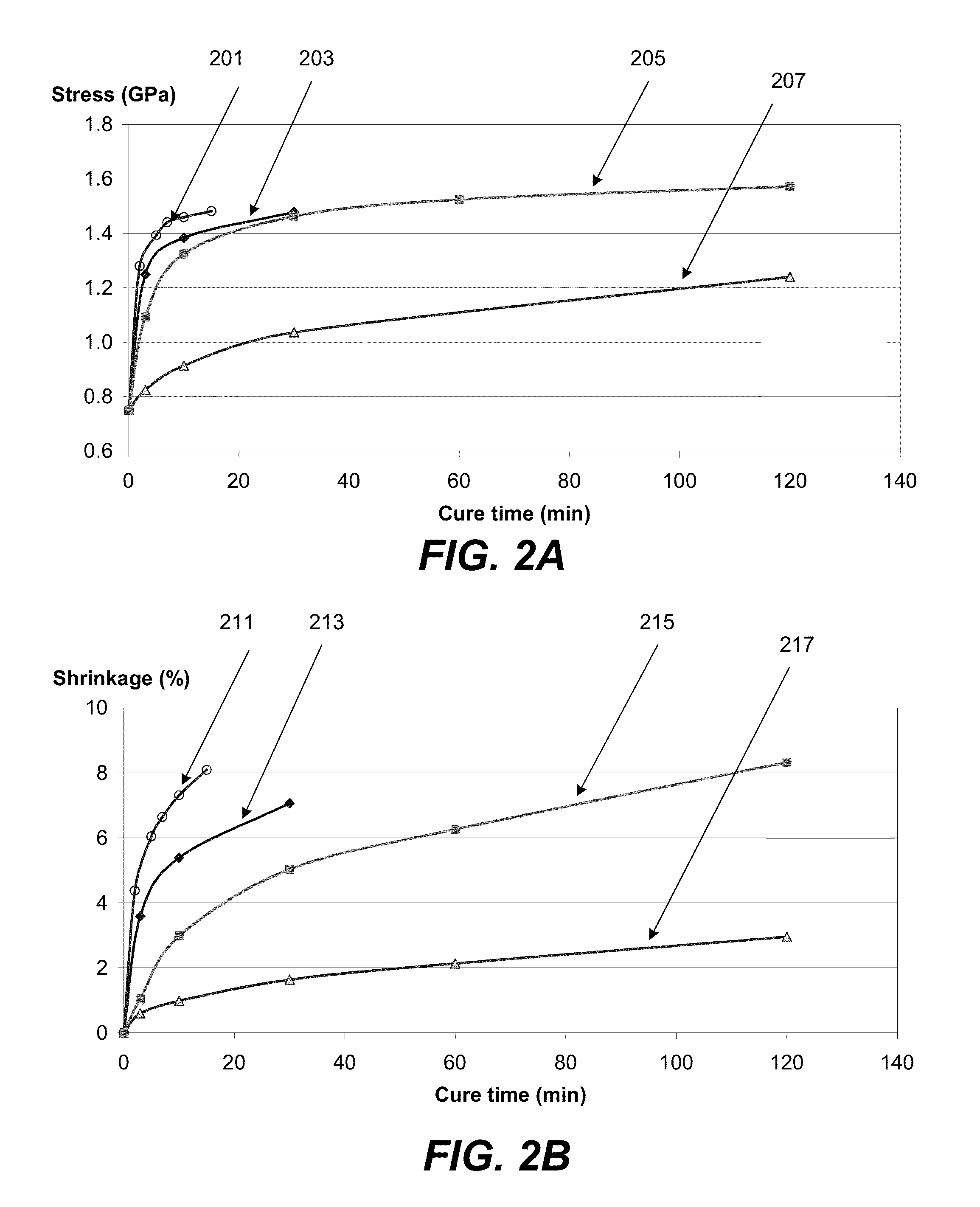
This approach allows for the achievement of tensile stresses exceeding 1.65 GPa at temperatures below 480°C, enabling improved transistor performance by inducing strain in NMOS channels while maintaining substrate integrity.

Problems solved by technology

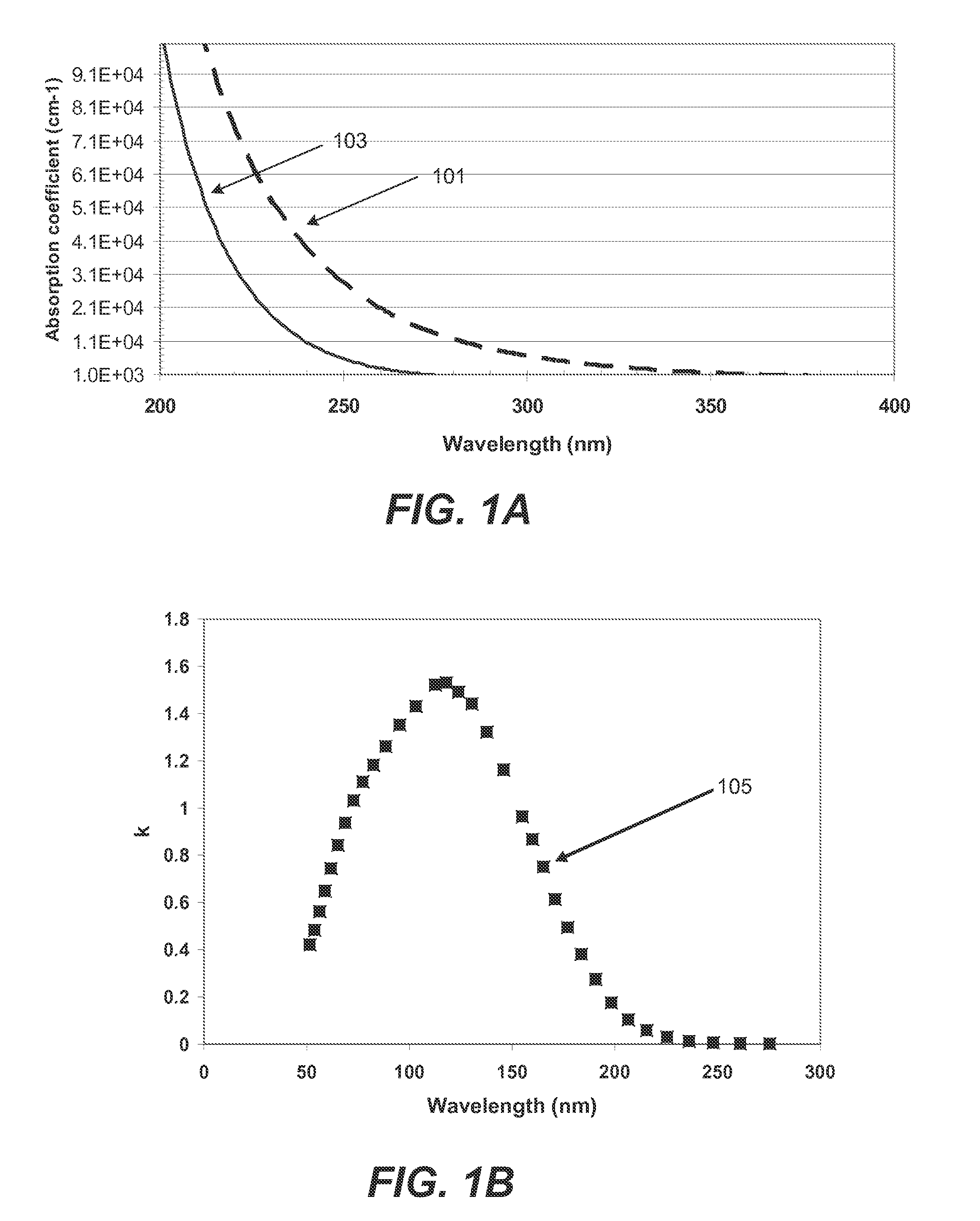
UV curing of as-deposited PECVD silicon nitride films, for example, has been shown to bring about significant hydrogen removal and shrinkage, resulting in tremendous stress changes.

Method used


Image

  • Cascaded cure approach to fabricate highly tensile silicon nitride films
  • Cascaded cure approach to fabricate highly tensile silicon nitride films
  • Cascaded cure approach to fabricate highly tensile silicon nitride films

Examples


Embodiment Construction

[0028]Reference will now be made in detail to specific embodiments of the invention. Examples of the specific embodiments are illustrated in the accompanying drawings. While the invention will be described in conjunction with these specific embodiments, it will be understood that it is not intended to limit the invention to such specific embodiments. On the contrary, it is intended to cover alternatives, modifications, and equivalents as may be included within the spirit and scope of the invention as defined by the appended claims. In the following description, numerous specific details are set forth in order to provide a thorough understanding of the present invention. The present invention may be practiced without some or all of these specific details. In other instances, well known process operations have not been described in detail in order not to unnecessarily obscure the present invention.

INTRODUCTION

[0029]The present invention provides a processing technique to generate a hi...


PUM

PropertyMeasurementUnit
temperatureaaaaaaaaaa
wavelength rangeaaaaaaaaaa

Abstract

A highly tensile dielectric layer is generated on a heat sensitive substrate while not exceeding thermal budget constraints. Cascaded ultraviolet (UV) irradiation is used to produce highly tensile films to be used, for example, in strained NMOS transistor architectures. Successive UV radiation of equal or shorter wavelengths with variable intensity and duration selectively breaks bonds in the Si—N matrix and minimizes shrinkage and film relaxation. Higher tensile stress than a non-cascaded approach may be obtained.

Description

CROSS REFERENCE TO RELATED APPLICATION[0001]This application is a continuation of and claims priority to U.S. patent application Ser. No. 11 / 897,838, now U.S. Pat. No. 8,211,510, filed Aug. 31, 2007 and titled “CASCADED CURE APPROACH TO FABRICATE HIGHLY TENSILE SILICON NITRIDE FILMS,” all of which is incorporated herein by this reference in its entirety.FIELD OF THE INVENTION[0002]This invention relates to electronic devices and associated fabrication processes. More specifically, the invention relates to highly tensile dielectric films on heat sensitive substrates formed by UV curing, for example implemented in strained transistor architecture for NMOS devices in which a highly tensile silicon nitride capping layer is provided on the source and drain regions to induce tensile strain in the NMOS channel region.BACKGROUND OF THE INVENTION[0003]As transistors are scaled to smaller dimensions there is a need for higher switching speeds. One solution to increase transistor speed is to s...

Claims


Application Information

Patent Timeline
Patent Type & Authority Patents(United States)
IPC IPC(8): B05D3/06
CPCC23C14/0652C23C16/345C23C16/56H01L21/0217H01L21/0231H01L21/3105H01L29/7843
Inventor VARADARAJAN, BHADRIJIANG, GENGWEIREDDY, SIRISH K.SIMS, JAMES S.
Owner NOVELLUS SYSTEMS
Learn More