Fin field effect transistor with variable channel thickness for threshold voltage tuning

a technology of threshold voltage and transistor, which is applied in the direction of transportation and packaging, radio frequency control devices, railway signalling, etc., can solve the problems of short channel effect, short channel effect, punch-through, and current leakage, and the critical importance of manufacturing reliability and cos

Active Publication Date: 2013-08-20
GLOBALFOUNDRIES U S INC
View PDF11 Cites 33 Cited by
  • Summary
  • Abstract
  • Description
  • Claims
  • Application Information

AI Technical Summary

Problems solved by technology

In addition to performance characteristics, performance reliability, and durability of devices, manufacturing reliability and cost are also critical.
Several problems may arise with the miniaturization of devices, including short channel effects, punch-through, and current leakage.
These problems affect both the performance of the devices and the manufacturing process.
However, variation of the threshold voltages across a large number of FINFETs on a single substrate may present difficulties.
The threshold voltage may be modulated by tuning the FINFET gate stack workfunctions (WF), but gate stack patterning to tune the WF in gate-first FINFET fabrication is challenging, and the choice of gate metals that results in different WFs that may be used in gate-last processing is relatively limited.

Method used


Image

  • Fin field effect transistor with variable channel thickness for threshold voltage tuning
  • Fin field effect transistor with variable channel thickness for threshold voltage tuning
  • Fin field effect transistor with variable channel thickness for threshold voltage tuning

Examples


Embodiment Construction

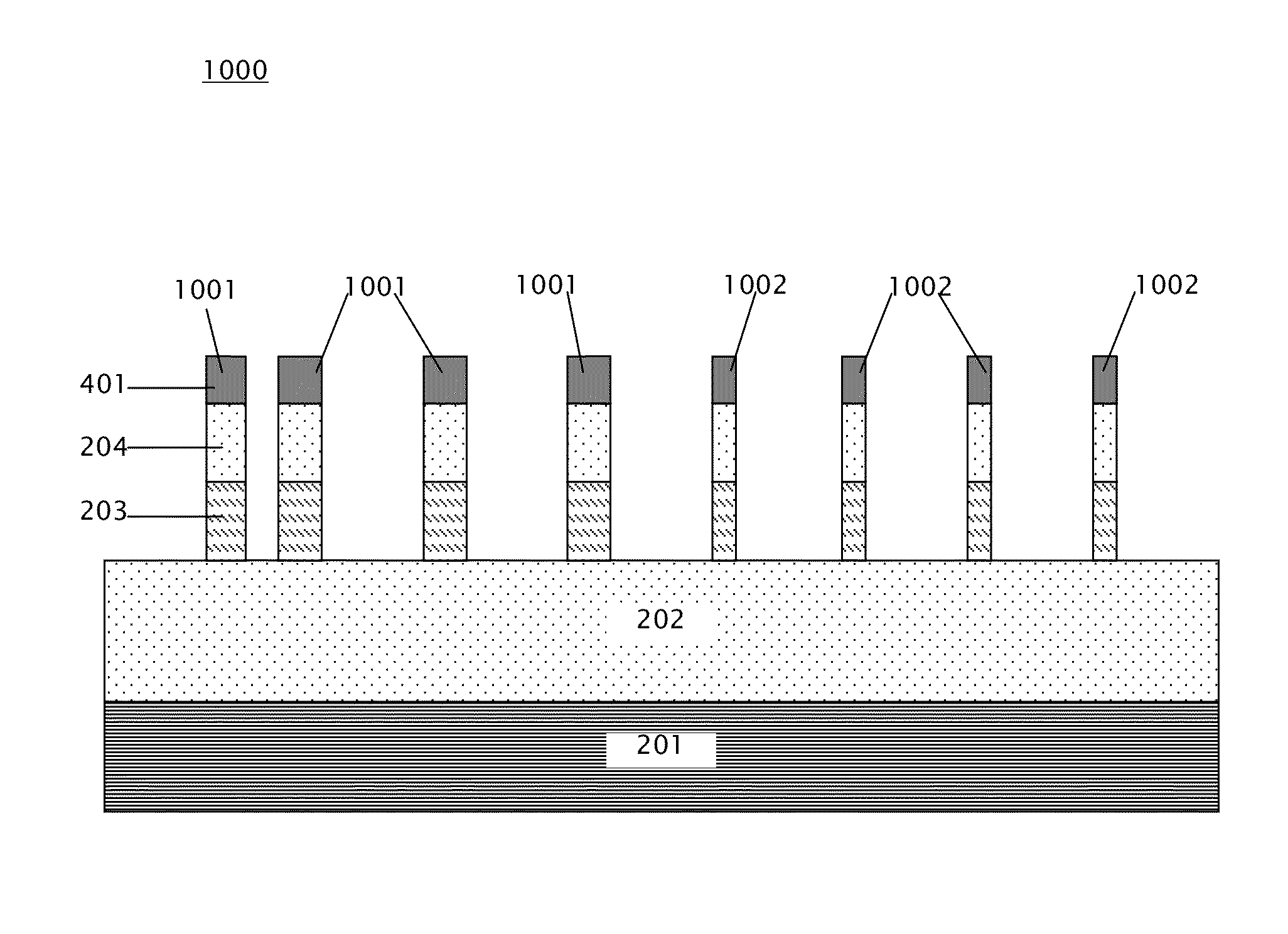
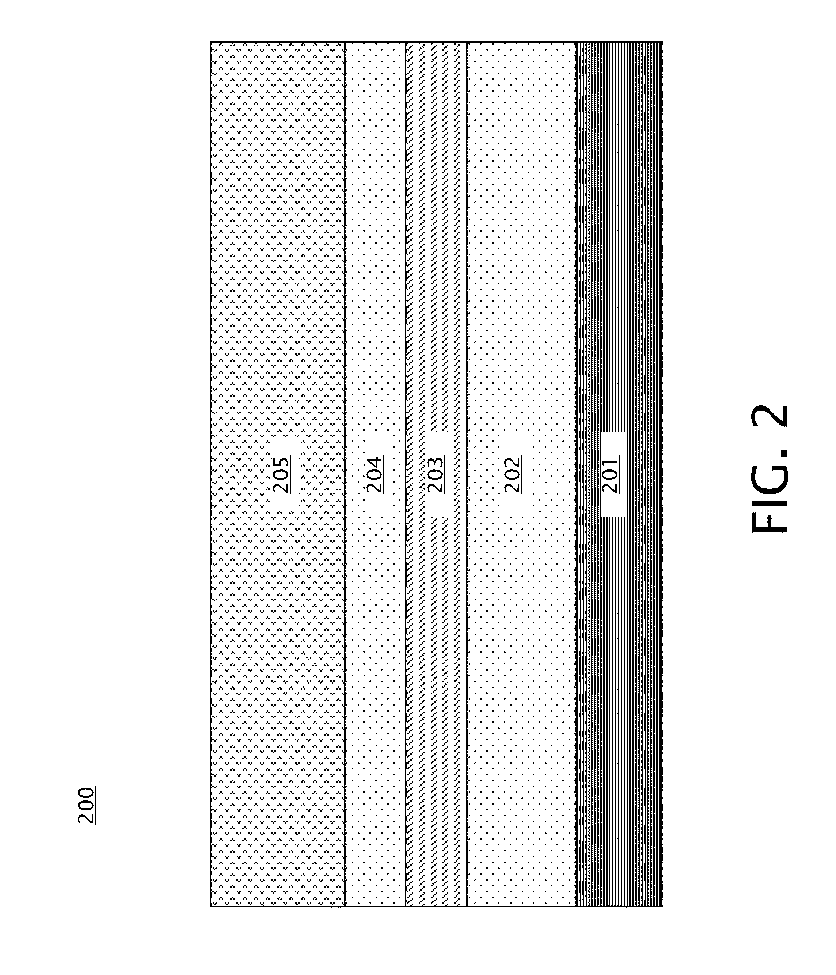
[0020]Embodiments of an IC that includes FINFETs having variable channel thicknesses for threshold voltage tuning, and methods of forming an IC that includes FINFETs having variable channel thicknesses for threshold voltage tuning, are provided, with exemplary embodiments being discussed below in detail. The threshold voltage of a FINFET device may be tuned by varying the thickness of the silicon that makes up the FINFET channel, which is in turn dependent on the thickness of the FINFET fin. Therefore, a plurality of FINFETs on a substrate may be formed with fin thicknesses, giving a range of device threshold voltages in a single IC. The threshold voltages of the different FINFET devices on the single substrate may be tuned across a range of about 100 millivolts (mV) or more in some embodiments, allowing for a wide variety of different IC design purposes.

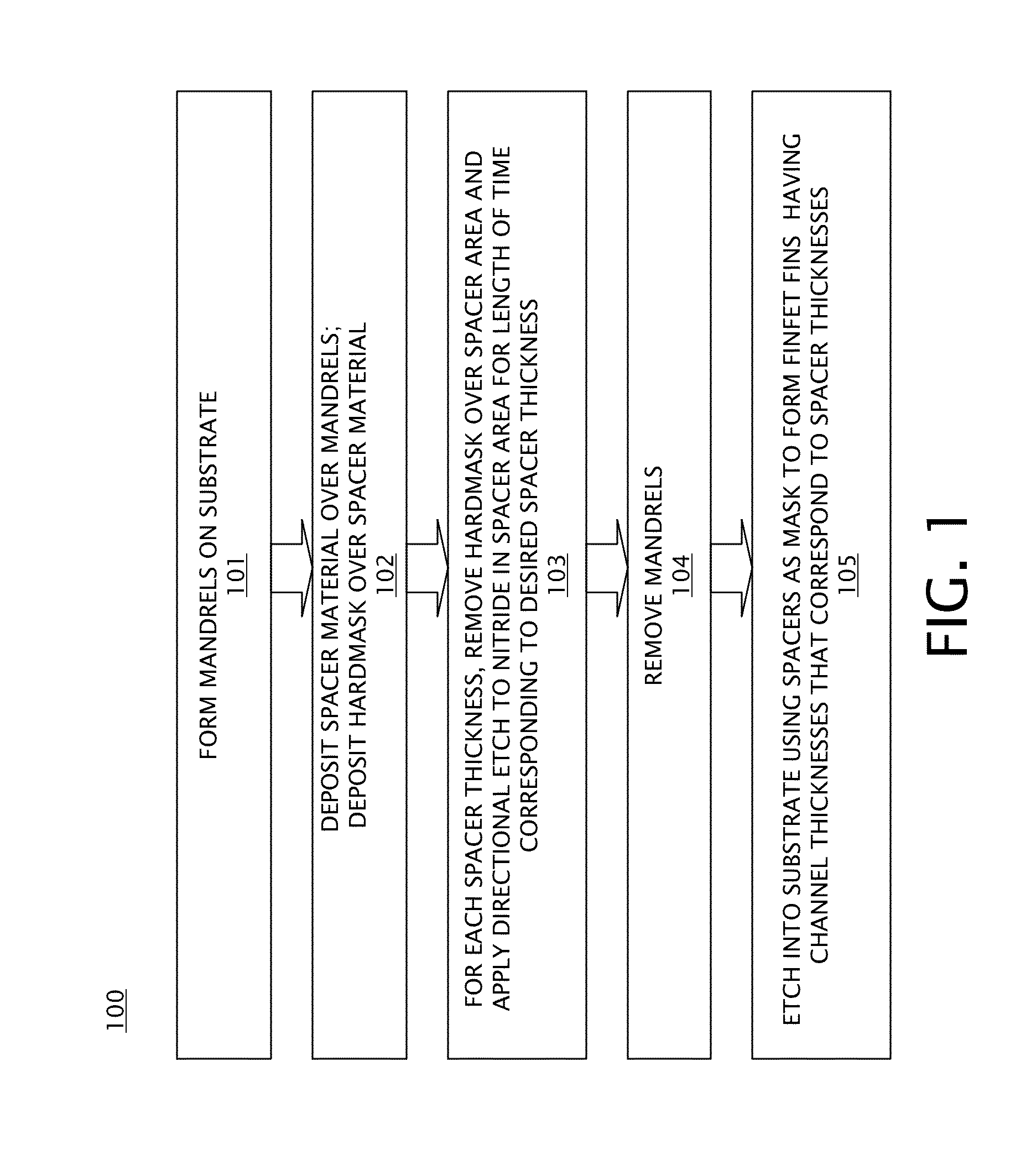
[0021]To form FINFETs having a range of fin thicknesses, spacers having varied thicknesses corresponding to the desired range of f...


PUM


Abstract

A method of forming an integrated circuit (IC) includes forming a first and second plurality of spacers on a substrate, wherein the substrate includes a silicon layer, and wherein the first plurality of spacers have a thickness that is different from a thickness of the second plurality of spacers; and etching the silicon layer in the substrate using the first and second plurality of spacers as a mask, wherein the etched silicon layer forms a first plurality and a second plurality of fin field effect transistor (FINFET) channel regions, and wherein the first plurality of FINFET channel regions each have a respective thickness that corresponds to the thickness of the first plurality of spacers, and wherein the second plurality of FINFET channel regions each have a respective thickness that corresponds to the thickness of the second plurality of spacers.

Description

BACKGROUND[0001]This disclosure relates generally to the field of semiconductor fabrication, and more particularly to threshold voltage tuning for fin field effect transistors (FINFET) on a substrate through variation of the FINFET channel thicknesses.[0002]Integrated circuits (ICs) may include large numbers of devices on a single substrate. As the number of devices formed per IC substrate and the density of the devices on the substrate increases, the dimensions of the individual devices drops significantly. In particular, the dimensions of gate thickness and channel separation of source and drain elements of field effect transistor (FET) devices may be reduced such that micrometer and nanometer separations of the source, drain, and gate in the substrate are required. Although devices are being steadily reduced in size, the performance characteristics of the devices must be maintained or improved. In addition to performance characteristics, performance reliability, and durability of...

Claims


Application Information

Patent Timeline
Patent Type & Authority Patents(United States)
IPC IPC(8): H01L21/311
CPCH01L21/3086H01L21/845H01L27/1211H01L27/0886
Inventor CAI, MINGGUO, DECHAOLIN, CHUNG-HSUNYEH, CHUN-CHEN
Owner GLOBALFOUNDRIES U S INC
Why Eureka
Try Eureka