
Plasma processing method and plasma processing apparatus

a plasma processing and plasma technology, applied in the field of plasma processing methods and plasma processing apparatuses, can solve the problems of reducing the potential difference between the wall of the processing chamber and the plasma (vwallvplasma), increasing the sputtering force of ions in the plasma on the wall surface, and affecting the production of components, etc., to achieve the effect of increasing the sheath voltage of the wall surface side, reducing the potential difference between the wall of the processing chamber and the plasma

Active Publication Date: 2013-10-01
TOKYO ELECTRON LTD
View PDF6 Cites 6 Cited by
  • Summary
  • Abstract
  • Description
  • Claims
  • Application Information

AI Technical Summary

Benefits of technology

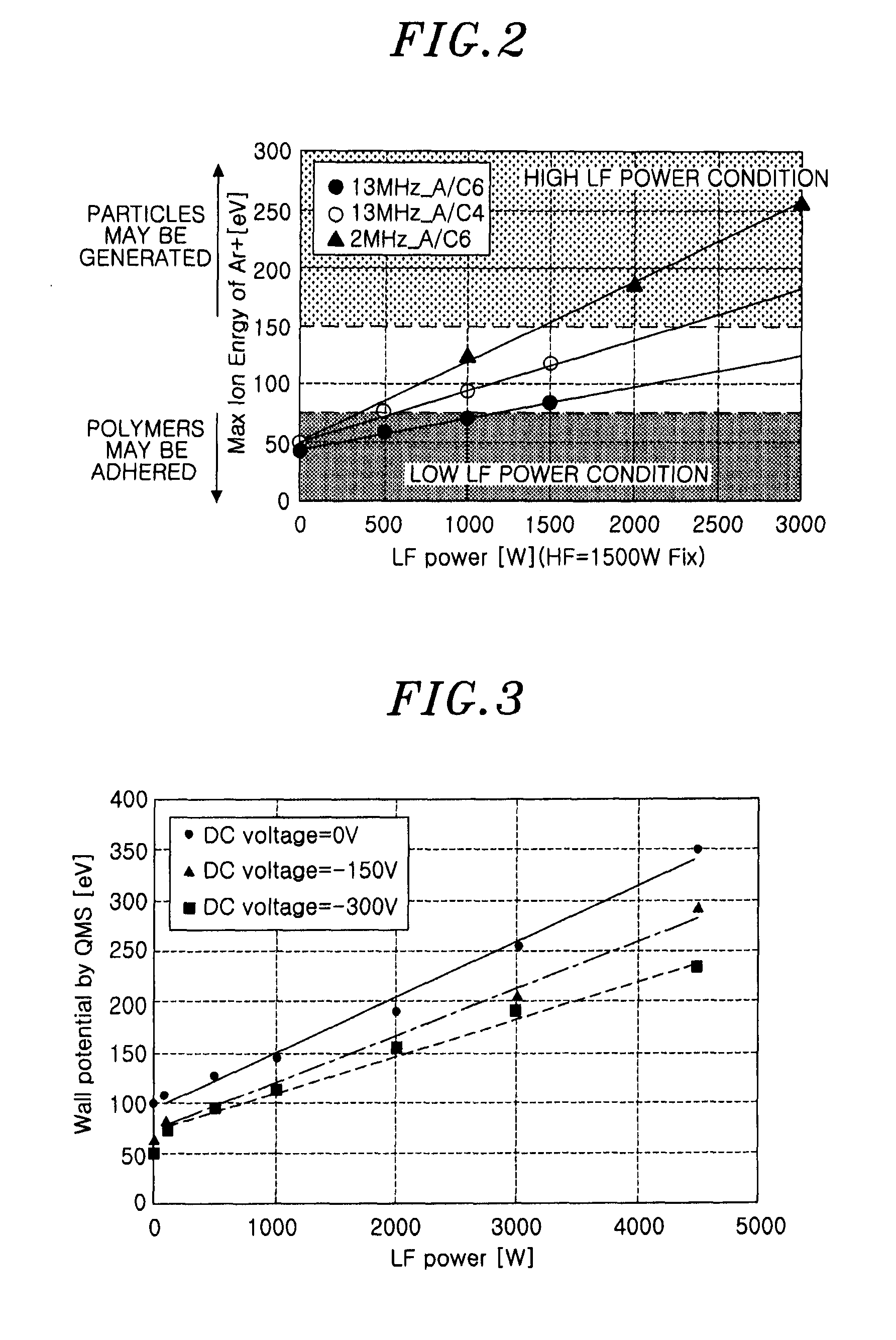
[0015]From the above, the inventors of the present invention have found that the potential difference between the wall of the processing chamber and the plasma (Vwall−Vplasma) is decreased when the DC voltage outputted from the DC power supply is applied to the auxiliary electrode, and is increased when the high frequency power outputted from the high frequency power supply is applied to the auxiliary electrode.
[0016]Hence, in the process in which the reaction products are easily deposited on the wall, the high frequency power outputted from the high frequency power supply is applied to the auxiliary electrode. Thus, the potential difference between the wall of the processing chamber and the plasma (Vwall−Vplasma) is increased, and a sheath voltage of the wall surface side is increased. This facilitates the acceleration of the ions in the sheath region of the wall surface side and increases the collision force of the ions with the wall. As a result, the deposition of the reaction products on the wall can be suppressed.
[0017]Meanwhile, in the process in which the wall is easily eroded, the DC voltage outputted from the DC power supply is applied to the auxiliary electrode. Hence, the potential difference between the wall of the processing chamber and the plasma (Vwall−Vplasma) is decreased, and a sheath voltage of the wall surface side is decreased. This decreases the acceleration of the ions in the sheath region of the wall surface side and decreases the collision force of the ions with the wall. As a consequence, the erosion of the wall can be suppressed. The above configuration makes it possible to prevent the excessive erosion of the wall and the excessive deposition of the deposits on the wall in the processing chamber.
[0018]In the above configuration, the potential-controlling high frequency power having a frequency lower than that of the plasma-exciting high frequency power is used, whereas the plasma-generating high frequency power is not used for the control of the wall potential. Therefore, the plasma-generating high frequency power can be set to a proper level in accordance with processes, and this allows the plasma to be maintained in a stable state. Further, in the above configuration, the auxiliary electrode is provided at a position located outer side of the target object while facing the mounting table. Accordingly, the wall potential control and the plasma generation control are separately carried out without affecting each other. As a result, the wall potential can be properly controlled while maintaining the plasma in a stable state.

Problems solved by technology

In other words, if the potential difference (Vwall−Vplasma) is too large, a sputtering force of ions in the plasma on the wall surface is increased, and radicals in the plasma may not be deposited easily on the wall surface.
Therefore, the wall of the processing chamber is eroded, and this causes production of particles, contamination in the chamber, erosion of components or the like.
Hence, components of the CF film adhered to the wall surface enter the plasma and react chemically with other substances, thereby inflicting adverse effects on a desired plasma process.
This is a so-called memory effect problem.
In addition to the memory effect problem, there is generated another problem in which the inside of the processing chamber needs to be cleaned frequently as the amount of the film adhered to the wall is increased.
This leads to a decrease in the productivity and an increase in the manufacturing cost.
When the high frequency power of a higher level is outputted from the high frequency power supply, a sputtering force on the wall surface is increased, and radicals are not easily deposited on the wall surface.
Therefore, the erosion amount of the wall is increased.
However, this technique cannot be used to solve the problem in which the wall is eroded or the film is formed on the wall during the plasma process.
When different processes are consecutively performed in a same processing chamber, the respective processes have different optimal high frequency power levels and, thus, it is extremely difficult to control the potential difference between the wall of the processing chamber and the plasma to be within a desired range under all the process conditions.
This causes an excessive increase or decrease of the potential difference between the wall and the plasma (Vwall−Vplasma), which results in an erosion of the wall or the deposition of the film on the wall.

Method used


Image

  • Plasma processing method and plasma processing apparatus
  • Plasma processing method and plasma processing apparatus
  • Plasma processing method and plasma processing apparatus

Examples


first embodiment

[0030](Entire Configuration of Plasma Processing Apparatus)

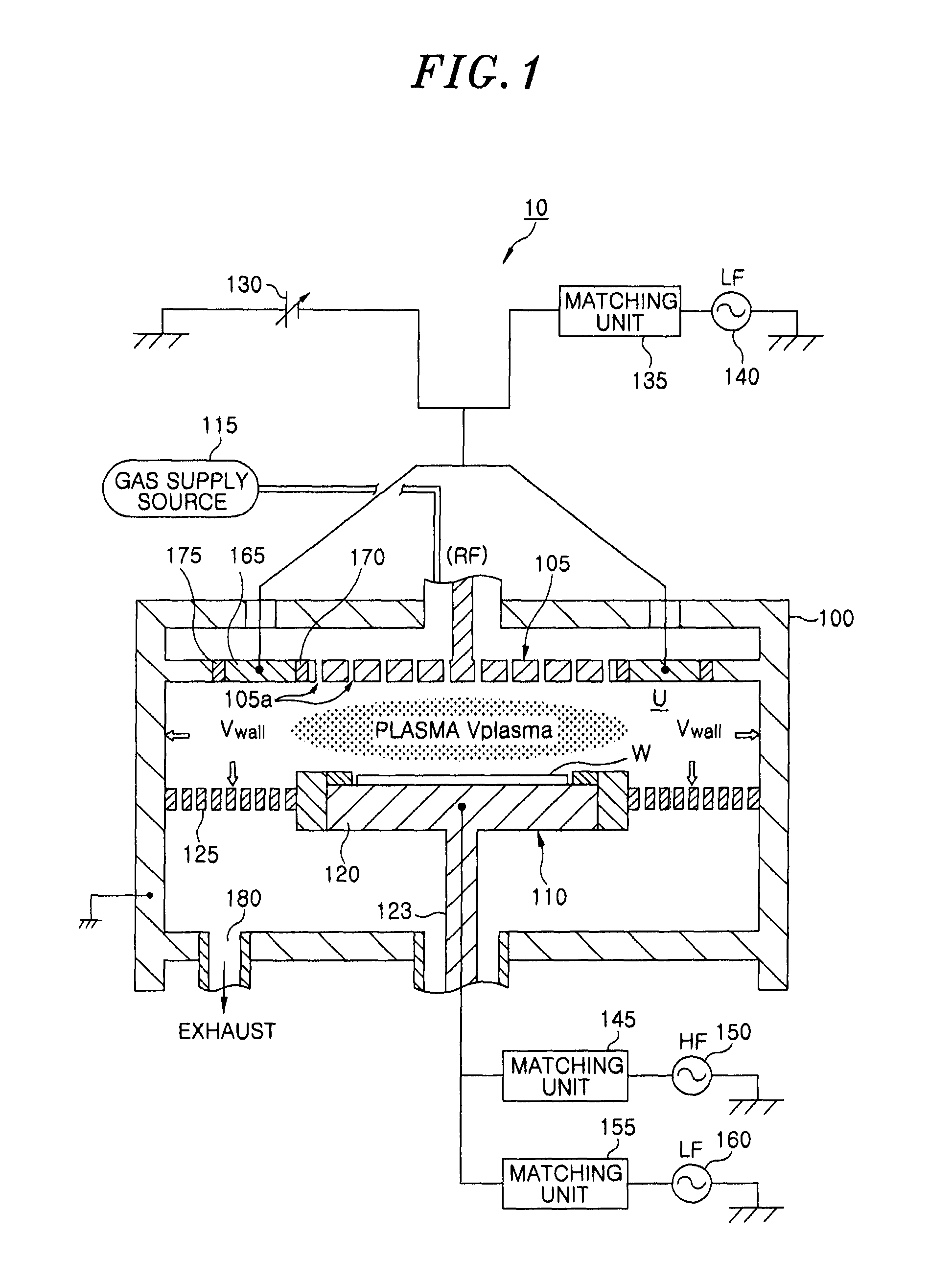
[0031]First of all, an entire configuration of a plasma processing apparatus in accordance with a first embodiment of the present invention will be described with reference to FIG. 1. FIG. 1 is a cross sectional view schematically showing a capacitively coupled (parallel plate type) etching apparatus in accordance with the present embodiment of the present invention. An etching apparatus 10 is an example of a plasma processing apparatus for plasma-processing a target object in a processing chamber.

[0032]The etching apparatus 10 includes a processing chamber 100 for plasma-processing a wafer W. The processing chamber 100 has a cylindrical shape and is grounded. The processing chamber 100 includes, e.g., a member obtained by thermally spraying an insulating material on an aluminum base, or a member obtained by coating silicon carbide on a silicon or an aluminum base.

[0033]An upper electrode 105 and a lower electrode 110 are di...

second embodiment

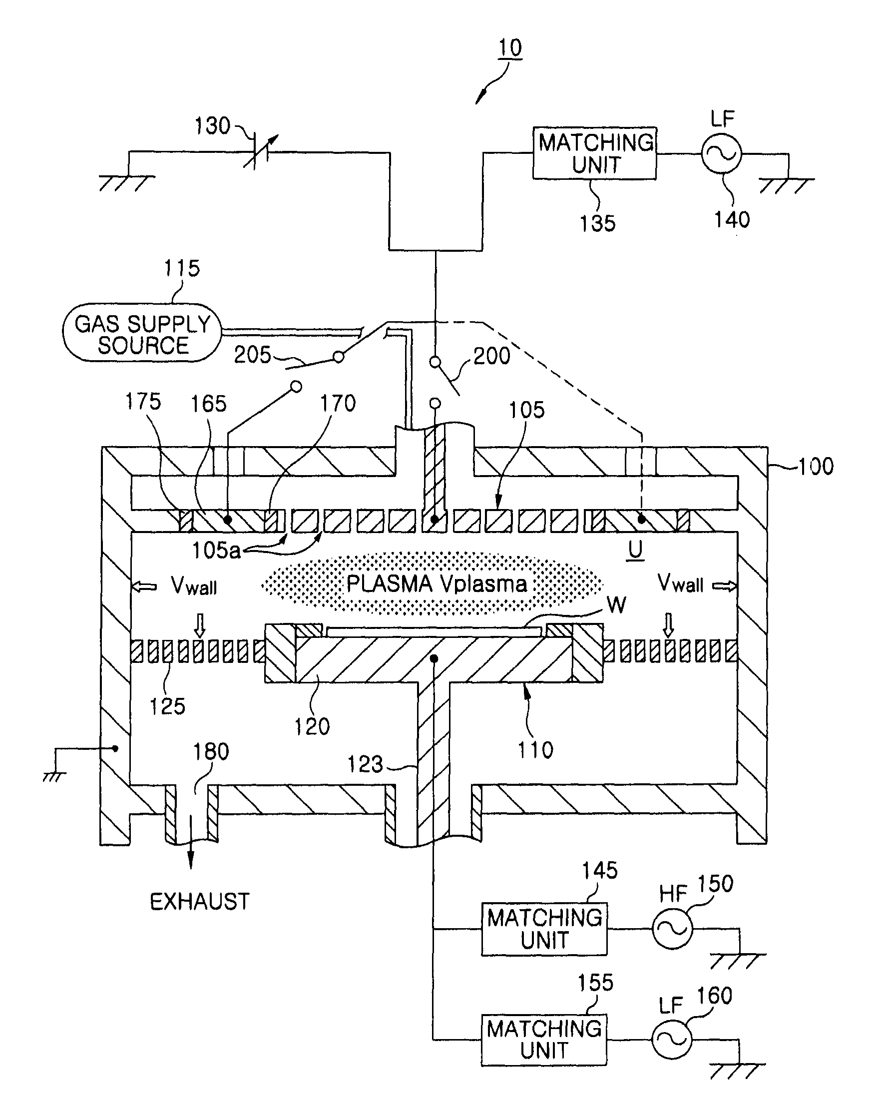
[0086]Hereinafter, an entire configuration of an etching apparatus in accordance with a second embodiment of the present invention will be described with reference to FIG. 5. The etching apparatus 10 of the second embodiment is different from that of the first embodiment in that the DC power supply 130 and the potential-controlling high frequency power supply 140 are connected to the upper electrode 105 and the auxiliary electrode 165. Therefore, only the difference will be described below, and the description on the configuration same as that of the first embodiment will be omitted.

[0087]The DC power supply 130 and the potential-controlling high frequency power supply 140 of the present embodiment are connected to the upper electrode 105 as well as the auxiliary electrode 165. A switch 200 is provided between the DC power supply 130 and the potential-controlling high frequency power supply 140 and the upper electrode 105. A switch 205 is provided between the DC power supply 130 and...

third embodiment

[0097]Hereinafter, an entire configuration of an etching apparatus in accordance with a third embodiment of the present invention will be described with reference to FIG. 6. In the etching apparatus 10 of the third embodiment, the high frequency bias power supply 160 for applying a bias voltage to the lower electrode 110 also serves as the supply source of the high frequency power applied to the auxiliary electrode 165. In view of this, the third embodiment is different from the first embodiment in which the supply source of the high frequency power applied to the auxiliary electrode 165 (the potential-controlling high frequency power supply 140) is provided in addition to the high frequency bias power supply 160. Hence, only the differences will be described below, and the description on the configuration same as that of the first embodiment will be omitted.

[0098]The present embodiment is not provided with the potential-controlling high frequency power supply 140 of the first embod...


PUM

PropertyMeasurementUnit
frequencyaaaaaaaaaa
frequencyaaaaaaaaaa
frequencyaaaaaaaaaa

Abstract

A plasma processing apparatus for generating a plasma in a plasma processing space in a processing chamber and plasma-processing a target object includes a plasma-exciting high frequency power supply for applying a plasma-exciting high frequency power. Further, the plasma processing apparatus includes at least one of a potential-controlling high frequency power supply for applying a potential-controlling high frequency power having a frequency lower than that of the plasma-exciting high frequency power and a DC power supply for applying a DC voltage; and a mounting table for mounting thereon a target object. Furthermore, the plasma processing apparatus includes an auxiliary electrode, provided at a position outer side of the target object mounted on the mounting table while facing the mounting table, connected to at least one of the potential-controlling high frequency power supply and the DC power supply.

Description

CROSS-REFERENCE TO RELATED APPLICATIONS[0001]This application claims priorities to Japanese Patent Application No. 2010-082918 filed on Mar. 31, 2010 and U.S. Provisional Application No. 61 / 327,122 filed on Apr. 23, 2010, the entire contents of which are incorporated herein by reference.FIELD OF THE INVENTION[0002]The present invention relates to a plasma processing method and a plasma processing apparatus for performing plasma process on a target object; and, more particularly, to a mechanism for controlling a wall potential.BACKGROUND OF THE INVENTION[0003]A plasma potential is higher than its surrounding potential. This will be explained by using as an example a parallel plate type plasma processing apparatus 99 shown in FIG. 8. In a plasma processing space in a processing chamber 900, when a bias potential is negative (negative wafer potential), i.e., when a wafer potential Vwafer is lower than a wall potential Vwall (i.e., ground), a plasma potential Vplasma becomes higher than...

Claims


Application Information

Patent Timeline
Patent Type & Authority Patents(United States)
IPC IPC(8): C23F1/00H01L21/306C23C16/00
CPCH01J37/32091H01J37/32165H01J37/32541H01J37/32568H01L21/02H01L21/0273H01L21/205H01L21/302H01L21/30621H01L21/3065H01L21/31116H01L21/76825H01L21/76826H05H1/46
Inventor HONDA, MASANOBU
Owner TOKYO ELECTRON LTD
Learn More