Method for reading NAND flash memory device using self-boosting

Active Publication Date: 2008-07-03
SK HYNIX INC
View PDF10 Cites 20 Cited by
  • Summary
  • Abstract
  • Description
  • Claims
  • Application Information

AI Technical Summary

Benefits of technology

[0014]In one embodiment, a method for reading a NAND flash memory device includes applying a first voltage to a first bit line coupled to a first cell string, the first cell string including a first string selection transistor, a plurality of first memory cells, and a first source selection transistor. A second voltage is applied to a second bit line coupled to a second cell string, the second cell string including a second string selection transistor, a plurality of second memory cells, and a second source selection transistor. The first and second string selection transistors are turned on. A read voltage is applied to a word line associated with one of the first memory cells that is selected for reading. A pass voltage is applied to a word line associated with one of the first memory cells that is not selected for reading. A state of the selected memory cell is determined according to a voltage condition associated with the first bit line. The second voltage applied to the second bit line reduces a potential difference between a gate and a channel of the unselected memory cell.

Problems solved by technology

In this case, a read disturb may also occur if the pass voltage Vpass applied to the word lines of memory cell transistors that are not selected exceeds a specific level.
Thus, the MLC structure causes a variety of problems such as performance degradation due to cycling.
However, if the pass voltage Vpass is increased the bias between the channels and the word lines of unselected memory cell transistors connected to the odd bit line BLo is also increased, raising the probability of a read disturb.

Method used


Image

  • Method for reading NAND flash memory device using self-boosting
  • Method for reading NAND flash memory device using self-boosting
  • Method for reading NAND flash memory device using self-boosting

Examples


Embodiment Construction

[0029]Embodiments of the present invention will now be described in detail with reference to the accompanying drawings. The embodiments of the present invention may be modified into various other forms and the scope of the present invention should not be construed as limited by the embodiments described below.

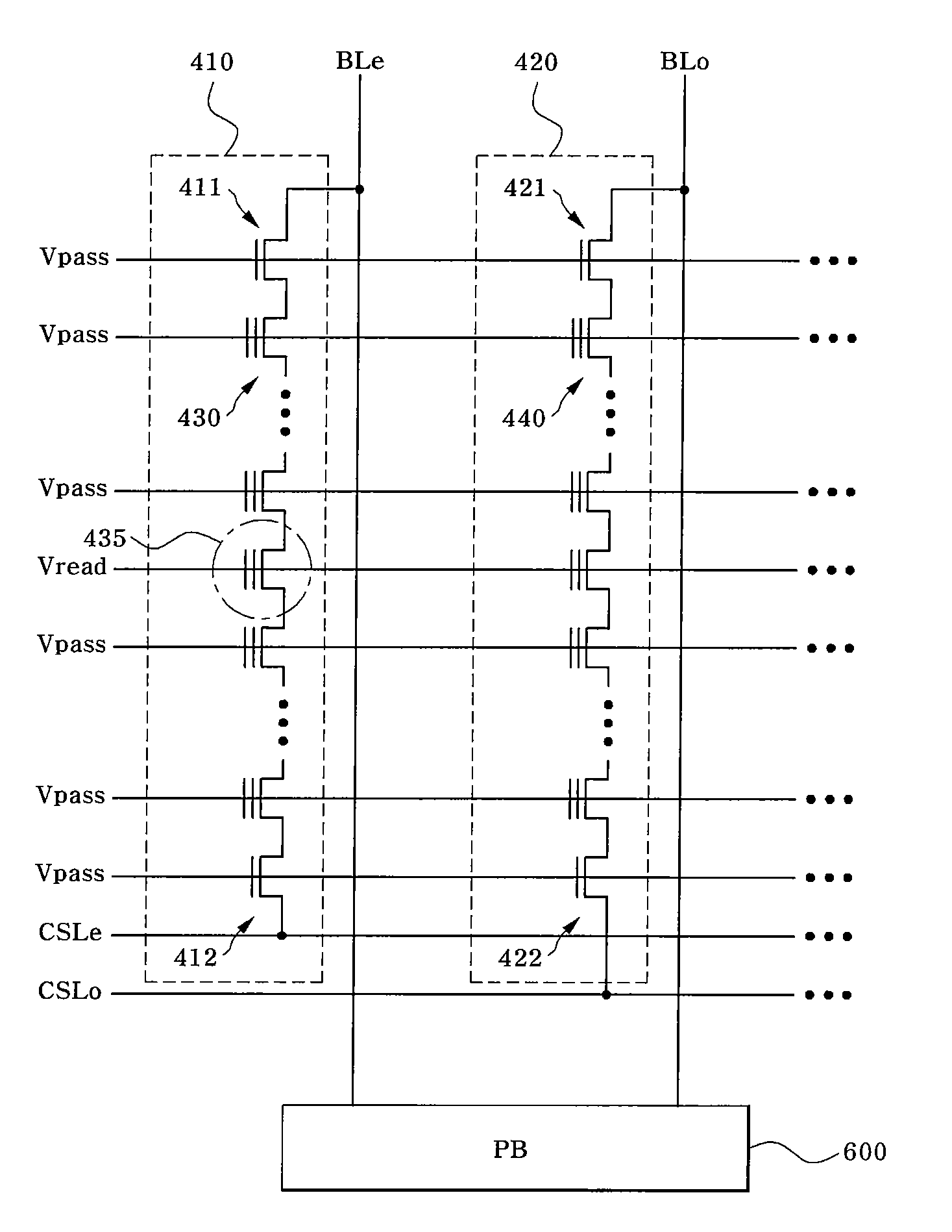
[0030]FIG. 4 illustrates a string structure of a NAND flash memory device to explain a method for reading a NAND flash memory device according to the present invention. As shown in FIG. 4, the NAND flash memory device has a memory cell array as a storage area to store data. The memory cell array includes a plurality of cell strings 410 and 420 that are connected to corresponding bit lines BLe and BLo. Of course, a number of cell strings are arranged in the memory cell array although only two cell strings 410 and 420 are shown in FIG. 4. Each of the cell strings 410 / 420 includes a string selection transistor 411 / 421 connected to a bit line BLe / BLo, a source selection transistor ...


PUM


Abstract

A method for reading a NAND flash memory device is provided. The NAND flash memory device includes a first bit line that is selected and a second bit line that is not selected. Each bit line is connected to a cell string including a string selection transistor, a plurality of memory cell transistors, and a source selection transistor connected in series. In the method, first, the first bit line is precharged while power supply voltage is applied to the second bit line. The string selection transistors are turned on and a read voltage is applied to a selected memory cell while a pass voltage is applied to unselected memory cells. The state of the selected memory cell transistor is detected according to whether or not charge precharged on the first bit line has been discharged.

Description

CROSS-REFERENCES TO RELATED APPLICATIONS[0001]The present application claims priority to Korean patent application number 10-2006-138809, filed on Dec. 29, 2006, which is incorporated by reference in its entirety.BACKGROUND OF THE INVENTION[0002]The present invention relates to a NAND flash memory device and more particularly to a method for reading a NAND flash memory device which reduces a read disturb that may occur during a read operation.[0003]Flash memory devices are widely used in a variety of electronic application fields in which nonvolatile memory devices are employed. A flash memory device typically uses a floating gate transistor as a unit cell and provides high memory density, high reliability, and low power consumption. Generally, flash memory devices are used in portable computers, personal digital assistants (PDAs), digital cameras, mobile phones, and the like. In addition, program code, system data such as a basic input / output system (BIOS), and firmware can also be...

Claims


Application Information

Patent Timeline
IPC IPC(8): G11C16/04G11C16/06
CPCG11C16/3418G11C16/0483G11C16/08G11C16/24G11C16/26
Inventor LEE, MIN KYU
Owner SK HYNIX INC
Why Eureka
Try Eureka