Organic material with a region including a guest material and organic electronic devices incorporating the same

a guest material and organic technology, applied in the direction of solid-state devices, semiconductor devices, coatings, etc., can solve the problems of low efficiency, low efficiency, and poor efficiency of organic electronic components formed using the ink diffusion process, so as to improve improve the effect of “gray-scale” intensity control and reduce the efficiency of such devices

Inactive Publication Date: 2005-05-12
EI DU PONT DE NEMOURS & CO
View PDF16 Cites 20 Cited by
  • Summary
  • Abstract
  • Description
  • Claims
  • Application Information

AI Technical Summary

Benefits of technology

[0136] Unexpectedly, the processes described above can be used to form localized doped regions in an organic layer before or after the organic layer is formed where the guest material concentration gradient between the opposite surfaces of an organic layer (near the electrodes) is smaller compared to conventional diffusion processes, and without the substantial lateral migration as seen with many conventional diffusion processes. A substantial amount, if not all, of the guest material migrates into the organic layer. The guest material can be “pulled” into the organic layer and obviate the need to perform a thermal diffusion process. Therefore, problems with too much lateral diffusion should not occur. Also, “partial” diffusions (through only part of the organic layer) or steep concentration gradients for guest material through the thickness of an organic layer should not occur.
[0137] Compare the new process to a conventional process. In one conventional process, a guest material is diffused from an ink outside the organic layer, and no more than about 25% of the guest material enters the organic layer. The concentrations of the guest material near the first and second electrodes using this conventional process may be anywhere from a few to several orders of magnitude different. In the new processes described herein, the guest material concentrations near the first and second electrodes should be less than an order of magnitude different, and possibly less than that. The lower concentration gradient allows the organic electronic component(s) to be operated over a larger potential difference without causing a shift in an emission or reception spectrum. Therefore, better “gray-scale” intensity control can be seen. Also, the organic electronic device can be operated at higher voltages as the efficiency of such device decreases with age without a significant shift in the emission spectrum.
[0138] Compare the new process to a convention diffusion process where the diffusion is performed until the guest material concentration gradient is close to zero (concentrations near opposite sides of the organic layer are substantially equal. This conventional diffusion process allows too much lateral diffusion and makes its use within a high resolution array very difficult.
[0139] If a guest material thermal drive step is used with the conventional ink diffusion process to reduce the guest material concentration gradient, the guest material may also laterally migrate to a point where it could interfere with the proper radiation emission or reception of adjacent organic electronic components. In a filter layer, the filter may have undesired filtering characteristics. Because the new processes do not use a guest material drive step, the amount of lateral migration of guest material is kept relatively low.
[0140] The new processes can be used to introduce guest materials into an organic active layer and still achieve good efficiencies because an ink diffusion process is not required. Efficiencies higher than 0.4 cd / A can be achieved. In one embodiment, the efficiency of a red-doped organic active region is at least 1.1 cd / A, the efficiency of a green-doped organic active region is at least 3.0 cd / A, and the efficiency of a blue-doped organic active region is at least 1.1 cd / A. Even higher efficiencies are possible.
[0141] The new process is not as sensitive to thickness as the conventional ink diffusion process. Because the guest material concentration gradient is lower, the volume of liquid compound(s) can be adjusted for different thicknesses. The process allows for more flexibility if a different thickness of the organic layer is desired. The conventional ink diffusion process is highly sensitive to thickness changes due to the steep concentration gradient. Again, a thermal diffusion processing step is not required with the new process.

Problems solved by technology

However, manufacture of full color displays usually requires certain modifications to procedures used in manufacture of monochromatic displays.
Many problems occur when using this process for organic electronic devices formed by such processes.
Second, the organic electronic components formed using this ink diffusion process have poor efficiency.
Due to lower efficiency, the organic electronic components formed using the ink diffusion process have intensities too low to be used for commercially-sold displays.
Third, the diffusion process causes a very non-uniform distribution of guest material concentration, resulting in a high concentration gradient (change in concentration divided by distance) between electrodes with an organic electronic device.
The high guest material concentration gradient makes the display nearly impossible to use, particularly over time.
Therefore, intensity control of a single color (i.e., “gray-scale”) is difficult because the emission spectrum shifts with a change in intensity, both of which are caused by a change in the potential difference between the first and second electrodes.
Fourth, the ink diffusion process is nearly impossible to use in manufacturing because of the sensitivity to thickness of the organic active layer 150.
Both processes suffer from similar problems previously described.
If the diffusion is long enough to make the concentration of a guest material more uniform throughout a thickness of the layer (i.e., reduce the concentration gradient between the electrodes), lateral diffusion will be too large and can result in low resolution because the pixels will need to be large.
Alternatively, if lateral diffusion can be kept at an acceptable level for high resolution, the doping concentration gradient throughout the thickness of the organic layer may be unacceptably large.
In some instances, both problems may occur (i.e., unacceptably large laterally diffusion while having too severe of a concentration gradient between the electrodes of the organic electronic device).

Method used


Image

  • Organic material with a region including a guest material and organic electronic devices incorporating the same
  • Organic material with a region including a guest material and organic electronic devices incorporating the same
  • Organic material with a region including a guest material and organic electronic devices incorporating the same

Examples


example 1

[0146] This Example demonstrates that appropriate manipulation of physical properties of the organic active layer and the liquid composition provides organic electronic components in an organic electronic device without the need for banks or wells.

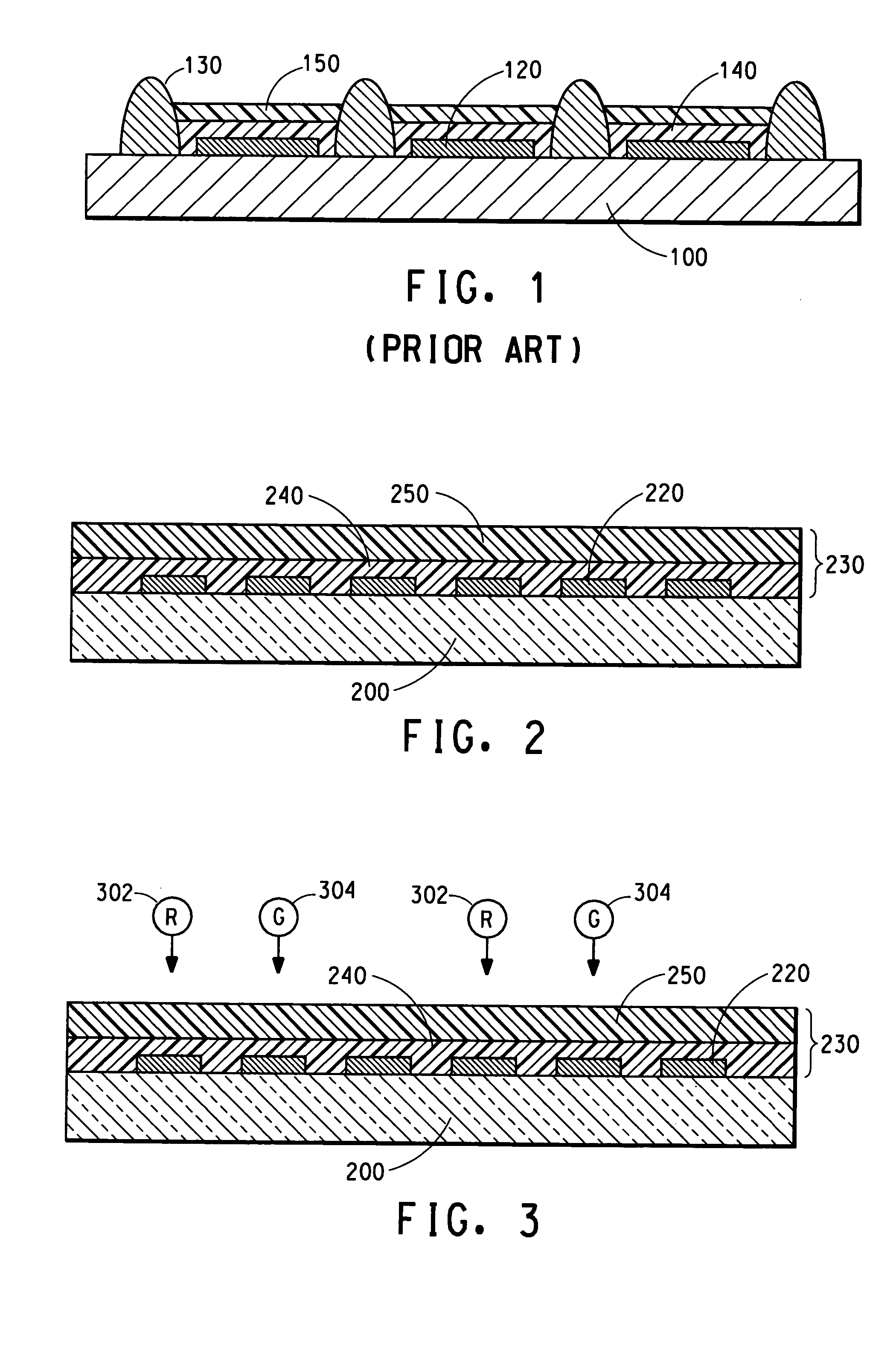
[0147] Organic electronic components are fabricated to include the following structure: ITO (first electrodes, or anodes) / buffer polymer / organic active / second electrode (cathode). The substrates are 30×30 mm (nominal) ITO coated glass. The charge transport layer is a PEDOT material (BAYTRON-P, Bayer AG, Germany). The organic active layers include a blue-emitting poly(spirobifluorene) material (a host material capable of emitting blue light without any guest materials). PEDOT is spin-coated onto a flat glass / ITO substrate at room temperature and then baked at approximately 200° C. for approximately 5 minutes. The film thickness is approximately 150 nm, as measured with a Dektec surface profiler. The blue-color organic active layer is then ...

example 2

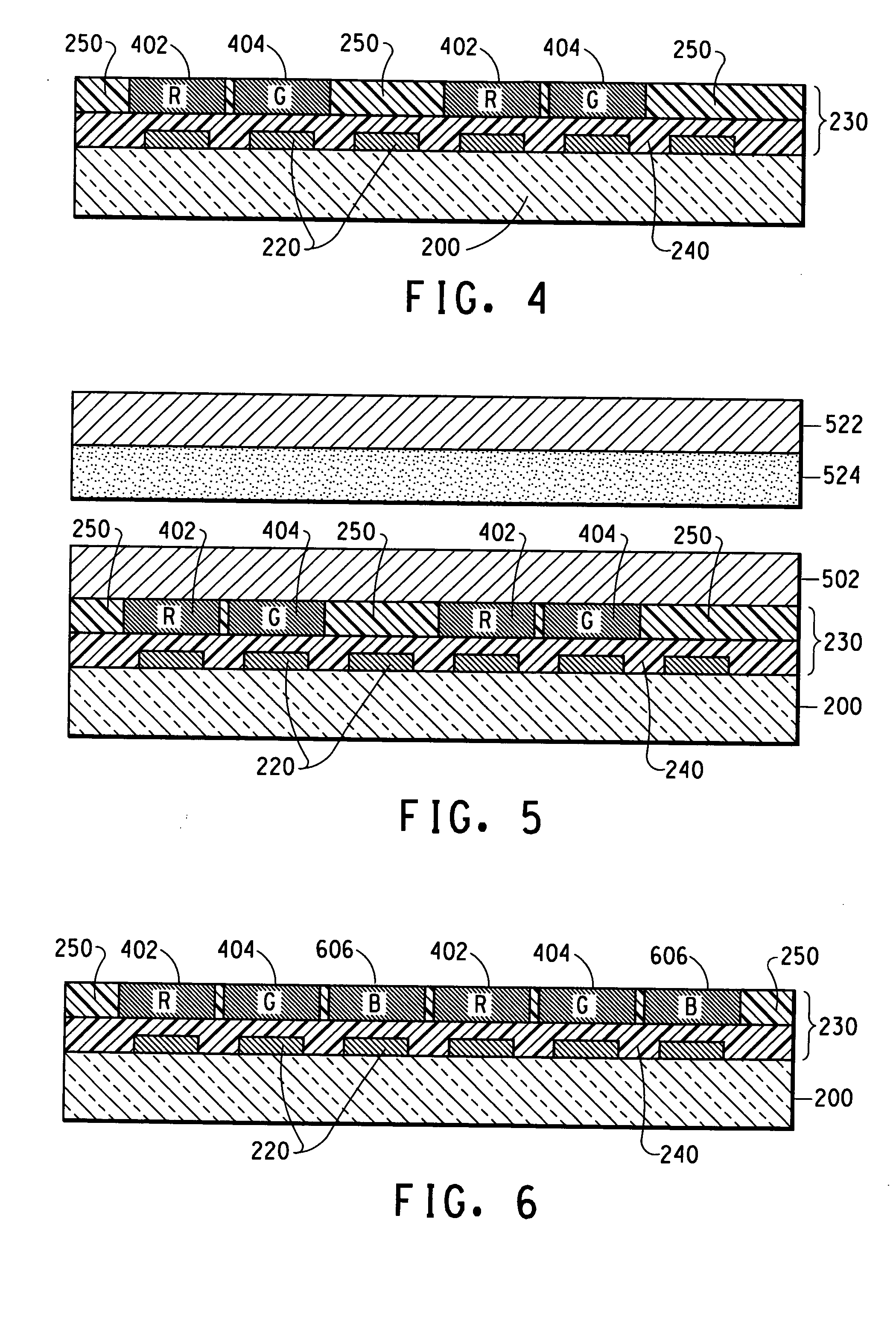
[0151] An experiment similar to Example 1 is performed, using a full-color display with 200 micron pixel pitch, nominal. The diameter of the ink jet nozzle is reduced to approximately 20 micron, and a display with multiple colors in a pre-defined pattern is produced using this smaller diameter nozzle. The diameter of the red or green emitting zones is reduced to approximately 65 micron. Thus, this example demonstrates that the processes described herein can be used to fabricate full color displays with less than a 200 micron pitch.

example 3

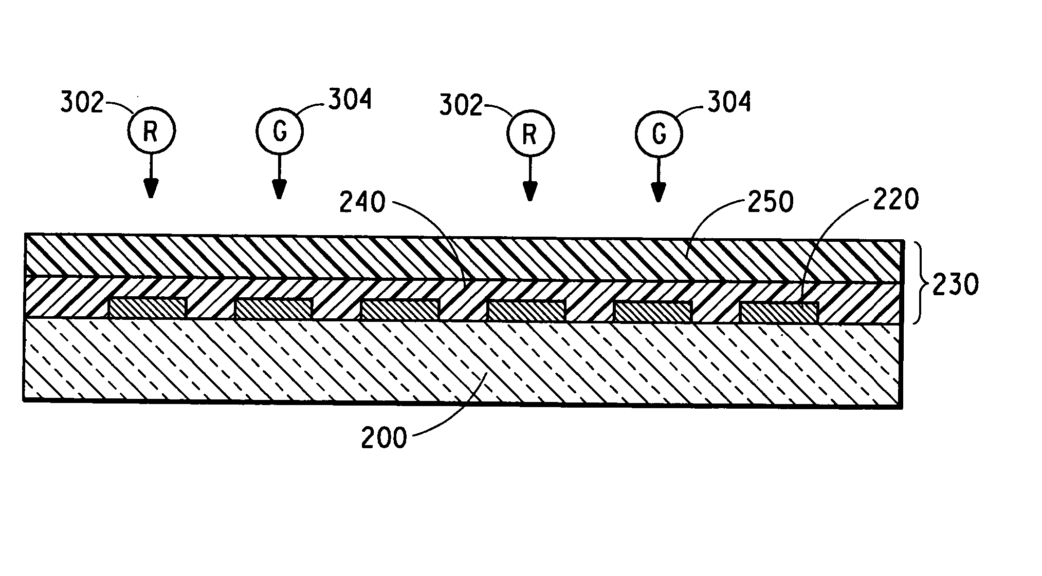
[0152] Full color displays with red, green and blue polymer lines are produced using a procedure similar to that described in Example 1. An ink-jet printer with 40 nozzles is used for defining color pixels. The diameter of these nozzles is approximately 35 microns and the step motion between each drop is approximately 85 microns. The substrate is 100 mm×100 mm (4 inch×4 inch), nominal with a display area of approximately 80 mm×60 mm (3.2 inch×2.4 inch). The substrate does not include any well structures. The red, green and blue color stripes indicate: (1) a line pattern can be achieved without using bank structures, and (2) a full-color display can be made with 100 pixels-per-inch (equivalent to 254 micron pitch).

[0153] Full color, active matrix displays are also fabricated with a substrate with thin-film-transistor pixel drivers. An organic active layer is constructed between the pixel drivers and the ITO contacts. As in Examples 1 and 2, bank structures are not required for color...


PUM

PropertyMeasurementUnit
temperatureaaaaaaaaaa
thickaaaaaaaaaa
FWHMaaaaaaaaaa

Abstract

Organic electronic devices may include an organic electronic component having an organic layer including guest material(s). One or more liquid compositions may be placed over a substantially solid organic layer. Each liquid composition can include guest material(s) and liquid medium (media). The liquid medium (media) may interact with the organic layer to form a solution, dispersion, emulsion, or suspension. The viscosity of the resulting solution, dispersion, emulsion, or suspension can be higher than the liquid composition to keep lateral migration of the guest material to a relatively low level. Still, most, if not all, the guest material(s) can migrate into the organic layer to locally change the electronic or electro-radiative characteristics of a region within the organic layer, with less than one order of magnitude difference in guest material concentration throughout the thickness of the organic layer. The process can be used for organic active layers, filter layers, and combinations thereof.

Description

FIELD OF THE INVENTION [0001] The invention relates generally to organic materials and organic electronic devices, and more specifically, to organic materials with regions including guest material(s) and processes for forming an organic layer and organic electronic devices incorporating such an organic layer and processes for using such devices. BACKGROUND OF THE INVENTION [0002] Organic electronic devices have attracted increasing attention in recent years. Examples of organic electronic device include Organic Light-Emitting Diodes (“OLEDs”). Current research in the production of full color OLEDs is directed toward the development of cost effective, high throughput processes for producing color pixels. For the manufacture of monochromatic displays, spin-coating processes have been widely adopted. However, manufacture of full color displays usually requires certain modifications to procedures used in manufacture of monochromatic displays. For example, to make a display with full col...

Claims


Application Information

Patent Timeline
Patent Type & Authority Applications(United States)
IPC IPC(8): H01L27/32H01L51/00H01L51/30H01L51/40H01L51/50H01L51/56
CPCC08G2261/3142C08G2261/5222H01L27/322H01L51/0004H01L51/56H01L51/0039H01L51/0052H01L51/5012H01L51/0037H10K59/38H10K71/13H10K85/115H10K85/1135H10K85/615H10K50/11H10K71/00H10K10/00
Inventor MACPHERSON, CHARLES DOUGLASSRDANOV, GORDANASTAINER, MATTHEWYU, GANG
Owner EI DU PONT DE NEMOURS & CO
Why Eureka
Try Eureka