Semiconductor device, method for manufacturing the same, and multilayer substrate having the same

a technology of semiconductor devices and multilayer substrates, applied in semiconductor devices, semiconductor/solid-state device details, electrical apparatus, etc., can solve problems such as difficult to improve completely difficulty, circuit malfunction, and difficulty in managing high voltage surges, so as to reduce displacement current generation

Active Publication Date: 2010-07-15
DENSO CORP
View PDF11 Cites 20 Cited by
  • Summary
  • Abstract
  • Description
  • Claims
  • Application Information

AI Technical Summary

Benefits of technology

[0009]In view of the above-described problem, it is an object of the present disclosure to provide a semiconductor device, a method for manufacturing the semiconductor device, and a multi layer substrate having a built-in semiconductor device, which includes a low potential reference circuit portion and a high potential reference circuit portion disposed on a same chip, and provides to reduce generation of a displacement current caused by a dv / dt surge for charging and discharging a parasitic capacitor.
[0011]In the above method, it is possible to reduce or preclude a potential difference between both ends of a parasitic capacitor formed in the semiconductor device, and therefore, a capacitance is cancelled. Thus, generation of a displacement current generated by a dv / dt surge for charging and discharging a parasitic capacitor is prevented. Further, it is possible to prevent malfunction of a circuit.
[0013]Thus, regarding the semiconductor device formed by the manufacturing method with using the bulk semiconductor substrate, it is possible to reduce or preclude a potential difference between both ends of a parasitic capacitor formed in the semiconductor device, and therefore, a capacitance is cancelled. Thus, generation of a displacement current generated by a dv / dt surge for charging and discharging a parasitic capacitor is prevented. Further, it is possible to prevent malfunction of a circuit.
[0015]Thus, it is possible to reduce or preclude a potential difference between both ends of a parasitic capacitor formed in the semiconductor device, and therefore, a capacitance is cancelled. Thus, generation of a displacement current generated by a dv / dt surge for charging and discharging a parasitic capacitor is prevented. Further, it is possible to prevent malfunction of a circuit.
[0017]Thus, it is possible to reduce or preclude a potential difference between both ends of a parasitic capacitor formed in the semiconductor device, and therefore, a capacitance is cancelled. Thus, generation of a displacement current generated by a dv / dt surge for charging and discharging a parasitic capacitor is prevented. Further, it is possible to prevent malfunction of a circuit.

Problems solved by technology

However, in the HVIC 107 having the high potential reference circuit and the low potential reference circuit made into one chip, interference of potential between the high potential reference circuit and the low potential reference circuit occurs, so that the circuit may malfunction.
It is difficult to manage this high voltage surge (defined as a dv / dt surge since voltage increase is high with respect to the rising edge period) having the rapid rising edge without malfunction of the circuit.
However, in the HVIC having the trench isolation structure with using the SOI substrate, the potential interferes through a support substrate when the dv / dt surge is applied so that displacement current for charging and discharging a parasitic capacitance formed by an insulation layer between the support substrate and a semiconductor layer (i.e., a SOI layer) is generated.
However, it is difficult to improve completely the difficulty since a tiny displacement current may cause the malfunction when an amplifier circuit having a large gain or the like is integrated.

Method used


Image

  • Semiconductor device, method for manufacturing the same, and multilayer substrate having the same
  • Semiconductor device, method for manufacturing the same, and multilayer substrate having the same
  • Semiconductor device, method for manufacturing the same, and multilayer substrate having the same

Examples


first embodiment

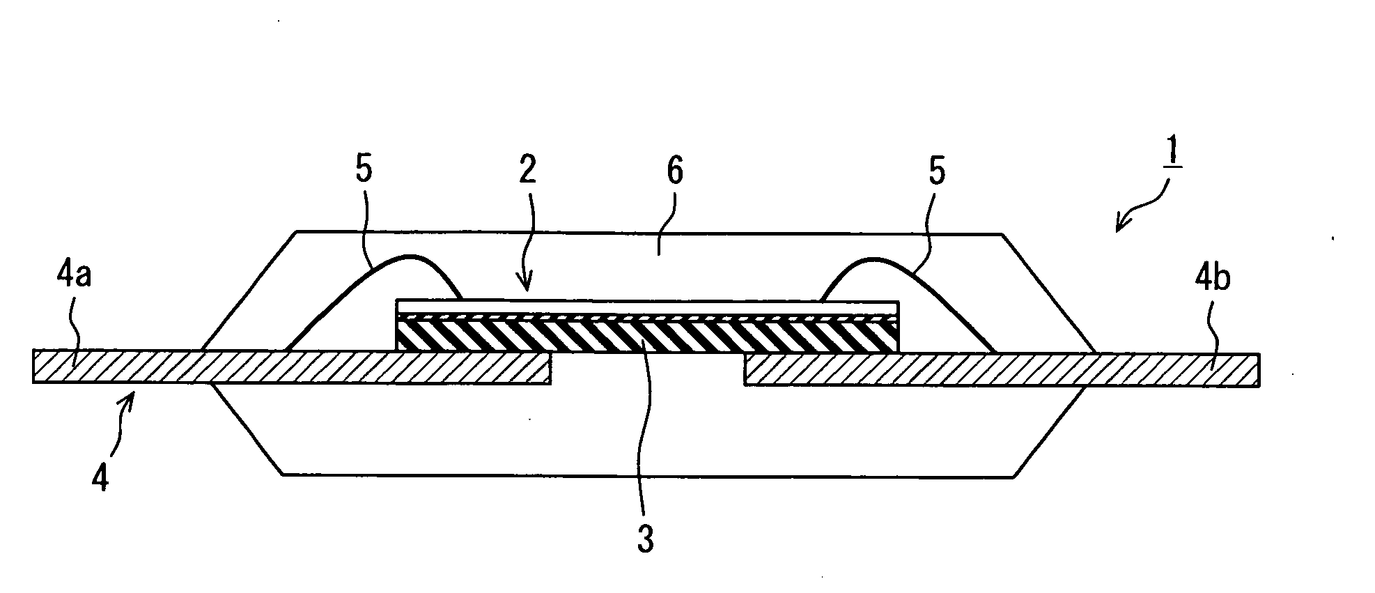
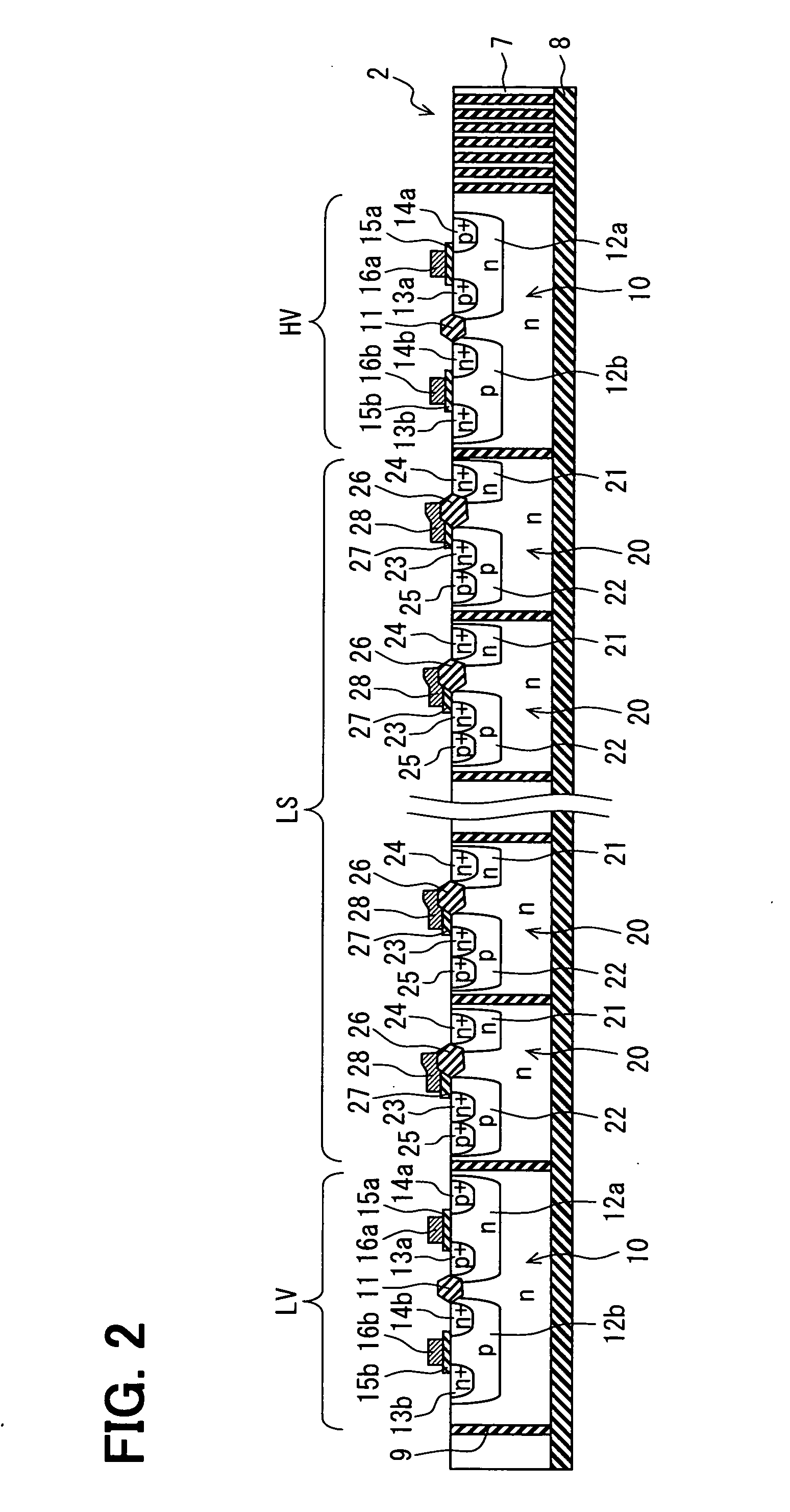
[0077]FIG. 1 is a cross sectional view showing a skeleton constitution of a semiconductor device according to a first embodiment. FIG. 2 is a cross sectional view showing a skeleton constitution of a semiconductor chip of the semiconductor device in FIG. 1. FIG. 3 is a layout diagram showing the semiconductor device shown in FIG. 1 seeing from an upper side. Here, in FIG. 3, a seal resin is not shown. Further, FIG. 2 corresponds to a cross sectional view taken along line II-II in FIG. 3.

[0078]A thickness direction of a semiconductor layer is simply defined as a thickness direction, and a direction perpendicular to the thickness direction is simply defined as a vertical direction.

[0079]As shown in FIG. 1, in the semiconductor device 1 of the present embodiment, a semiconductor chip 2 for providing a HVIC is fixed to a lead 4 through an insulation member 3. The HVIC on the semiconductor chip 2 has a certain portion, which is electrically coupled with the lead 4 via a bonding wire 5. A...

second embodiment

[0122]Next, a second embodiment of the present invention will be explained with reference to FIGS. 10A to 10E. FIGS. 10A to 10E are cross sectional views showing a manufacturing process of a semiconductor device according to a second embodiment, FIG. 10A shows a state that a circuit portion forming step in a semiconductor substrate is completed, FIG. 10B shows a state that a step for bonding a support member is completed, FIG. 10C shows a state that a cutting step in a thinning process of a semiconductor substrate is completed, FIG. 10D shows a state that a polishing step in the thinning process of the semiconductor substrate is completed, and FIG. 10E shows a state that a step for fixing an insulation member is completed. In FIGS. 10A to 10E, the insulation isolation trench is shown, but the circuit portion LV, HV, LS (and their constitution elements), the wiring portion and the interlayer insulation film are not shown. Further, arrangement of the insulation isolation trench shown ...

third embodiment

[0136]Next, a third embodiment will be explained with reference to FIGS. 12 to 14. FIG. 12 is a plan view showing a skeleton constitution of a semiconductor device according to a third embodiment. FIG. 13 is a cross sectional view showing the semiconductor device taken along line XIII-XIII in FIG. 12. FIG. 14 is a pattern diagram showing an equipotential distribution in an insulation member in the semiconductor device shown in FIGS. 12 and 13. Here, FIG. 12 corresponds to FIG. 3, and FIG. 13 corresponds to FIG. 1. Further, FIG. 14 corresponds to FIG. 4. In FIGS. 12 to 14, only four third leads 4c (4c1-4c4) are shown as a matter of convenience.

[0137]In the first embodiment, the circuit portion LV, HV, LS is formed in the semiconductor layer 7. The first lead 4a is arranged to be opposite to the low potential reference circuit LV, and the second lead 4b is arranged to be opposite to the high potential reference circuit HV. On the other hand, in the present embodiment, as shown in FIGS...


PUM


Abstract

A method for manufacturing a semiconductor device includes: preparing a wafer formed of a SOI substrate; forming a circuit portion in a principal surface portion; removing a support substrate of the SOI substrate; fixing an insulation member on a backside of a semiconductor layer so as to be opposite to the circuit portion; dicing the wafer and dividing the wafer into multiple chips; arranging a first conductive member on the insulation member so as to be opposite to a part of the low potential reference circuit, and arranging a second conductive member on the insulation member so as to be opposite to a part of the high potential reference circuit; and coupling the first conductive member with a first part of the low potential reference circuit, and coupling the second conductive member with a second part of the high potential reference circuit.

Description

CROSS REFERENCE TO RELATED APPLICATIONS[0001]This application is based on Japanese Patent Applications No. 2009-6982 filed on Jan. 15, 2009, No. 2009-238483 filed on Oct. 15, 2009, and No. 2009-284343 filed on Dec. 15, 2009, the disclosures of which are incorporated herein by reference.FIELD OF THE INVENTION[0002]The present invention relates to a semiconductor device, a method for manufacturing the same, and a multi-layer substrate having a built-in semiconductor device.BACKGROUND OF THE INVENTION[0003]One of semiconductor devices used for an inverter control to drive a load such as a motor is a HVIC (high voltage integrated circuit). The HVIC controls a power device accommodated in an inverter for driving a load.[0004]Conventionally, as shown in FIG. 55, a HVIC 107 is used for driving the inverter. The HVIC 107 includes a high potential reference gate driving circuit 103, a low potential reference gate driving circuit 104, level shift elements 105a, 105b and a control circuit 106....

Claims


Application Information

Patent Timeline
Patent Type & Authority Applications(United States)
IPC IPC(8): H01L27/06H01L21/78
CPCH01L21/84H01L2924/1305H01L23/4951H01L23/49551H01L24/73H01L2224/48091H01L2224/48227H01L2224/48247H01L2224/73257H01L2224/73265H01L2924/01004H01L2924/01013H01L2924/01033H01L2924/01078H01L2924/01079H01L2924/01082H01L2924/09701H01L2924/19041H01L23/3107H01L2924/1306H01L2224/83191H01L24/27H01L2924/13055H01L2224/73204H01L2924/13091H01L2924/014H01L2924/01075H01L2924/01074H01L2924/01068H01L2924/01023H01L2924/01006H01L2924/01005H01L2224/32245H01L24/48H01L2924/00014H01L2924/00H01L2924/15788H01L2924/181H01L2924/14H01L2924/00012H01L2224/45099H01L2224/45015H01L2924/207
Inventor SENDA, KOUJISHIRAKI, SATOSHIMAEDA, YUKIHIROHIROSE, SHINICHIFUJII, TETSUONAKANO, TAKASHI
Owner DENSO CORP
Why Eureka
Try Eureka