Semiconductor light emitting device having heat dissipating vias

a technology of semiconductor light emitting device and heat dissipation via, which is applied in the direction of semiconductor devices, solid-state devices, lighting and heating apparatus, etc., can solve the problems of inability to provide desired intensity or chromaticity, disadvantageous die-bonding strength of leds, and variation of optical axes of leds from one to the other, so as to reduce the degree of influence of irregularities on the element mounting surface, improve heat dissipation performance of semiconductor light emi

Inactive Publication Date: 2013-10-01
STANLEY ELECTRIC CO LTD
View PDF8 Cites 2 Cited by
  • Summary
  • Abstract
  • Description
  • Claims
  • Application Information

AI Technical Summary

Benefits of technology

[0009]The invention has been made in view of the problems described above. An object of the invention is to provide a semiconductor light emitting device having high heat dissipation performance, large die-bonding strength of a portion where an LED is mounted, and a small amount of shift of the optical axis of the LED.
[0011]In the semiconductor light emitting device according to the invention, providing the heat dissipation via(s) passing through only the first ceramic layer and stacking the second ceramic layer on the first ceramic layer can prevent irregularities produced on the front surface of the first ceramic layer resulting from the formation of the heat dissipation vias from affecting the element mounting surface of the second ceramic layer. Since the heat dissipation via(s) does not overlap with the element mounting area of the second ceramic layer in the direction in which the first and second ceramic layers are stacked, the degree of influence of the irregularities on the element mounting surface can be further reduced. Moreover, providing the heat dissipation via(s) in a position(s) other than the portion immediately below the semiconductor light emitting element allows the second ceramic layer to be thinner, whereby the heat dissipation performance of the semiconductor light emitting device can be improved.
[0012]Further, reducing the magnitude of the irregularities described above can prevent the die-bonding strength of the semiconductor light emitting element from decreasing and the optical axis of the semiconductor light emitting element from shifting.

Problems solved by technology

A wiring substrate formed of a ceramic laminate, however, has another problem of irregularities on the front and rear surfaces resulting from heat dissipation vias.
When an LED is mounted on the glass layer with such large irregularities, the die-bonding strength of the LED disadvantageously decreases.
Further, the optical axis of the LED is shifted, and desired intensity or chromaticity cannot be provided.
Moreover, in a multi-chip-type semiconductor light emitting device in which a plurality of LEDs are mounted, such large irregularities produced on the surface of the glass layer disadvantageously cause the optical axes of the LEDs vary from one another.
Further, when the LEDs emit light of different colors, the color balance of the emitted light as a whole is disadvantageously degraded.

Method used


Image

  • Semiconductor light emitting device having heat dissipating vias
  • Semiconductor light emitting device having heat dissipating vias
  • Semiconductor light emitting device having heat dissipating vias

Examples


first embodiment

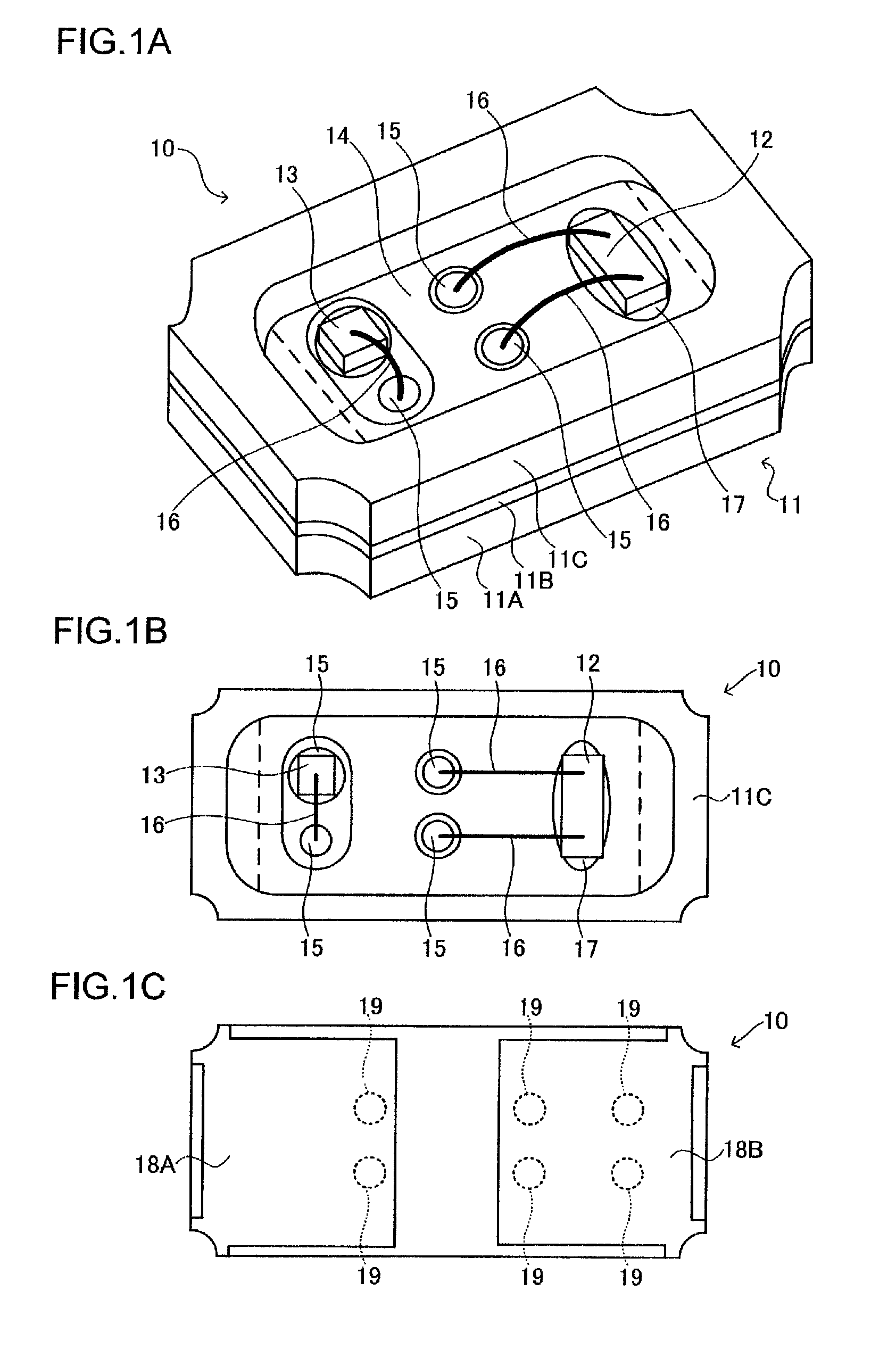
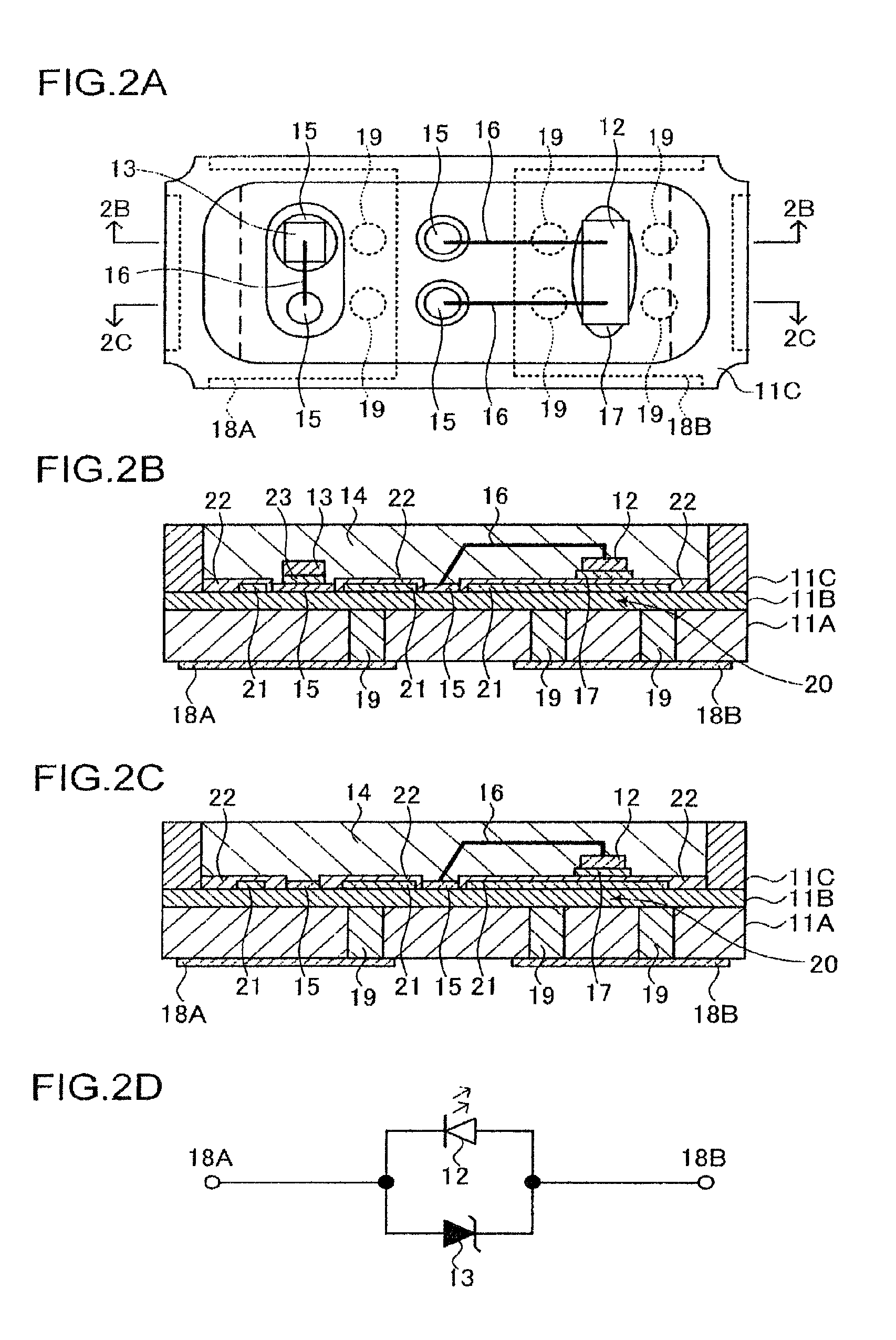
[0035]The structure of a semiconductor light emitting device according to a first embodiment of the invention will first be described with reference to FIGS. 1A to 1C and 2A to 2D. FIG. 1A is a perspective view of the semiconductor light emitting device according to the first embodiment of the invention. FIG. 1B is a plan view of the semiconductor light emitting device. FIG. 1C is a bottom view of the semiconductor light emitting device. FIG. 2A is a schematic plan view showing the positions of heat dissipation vias in the semiconductor light emitting device according to the first embodiment. FIG. 2B is a cross-sectional view taken along the line 2B-2B in FIG. 2A. FIG. 2C is a cross-sectional view taken along the line 2C-2C in FIG. 2A. FIG. 2D is an equivalent circuit diagram of the semiconductor light emitting device according to the first embodiment.

[0036]A semiconductor light emitting device 10 includes a wiring substrate 11 having a substantially rectangular shape in the plan vi...

second embodiment

[0058]In the first embodiment, the wiring pads 15 are formed on the second ceramic layer 11B. Alternatively, the wiring pads 15 may be formed on the first ceramic layer 11A. The positions where the wiring pads 15 are formed are thus changed in a second embodiment, which will be described with reference to FIGS. 5A to 5C. The same portions as those in the first embodiment have the same reference numerals, and only the portions different from those in the first embodiment will be described.

[0059]FIG. 5A is a plan view of a semiconductor light emitting device 100 according to the second embodiment of the invention. FIG. 5B is a cross-sectional view taken along the line 5B-5B in FIG. 5A. FIG. 5C is a cross-sectional view taken along the line 5C-5C in FIG. 5A.

[0060]A through hole 101 is formed through the second ceramic layer 11B, as shown in FIGS. 5A to 5C. The wiring pads 15 are formed on the first ceramic layer 11A exposed through the through hole 101. Employing the configuration desc...

third embodiment

[0062]The first and second embodiments have been described with reference to a semiconductor light emitting device having a single LED mounted therein. Alternatively, a plurality of LEDs may be mounted on the wiring substrate. A multichip-type semiconductor light emitting device in which a plurality of LEDs are mounted on the wiring substrate will be described below.

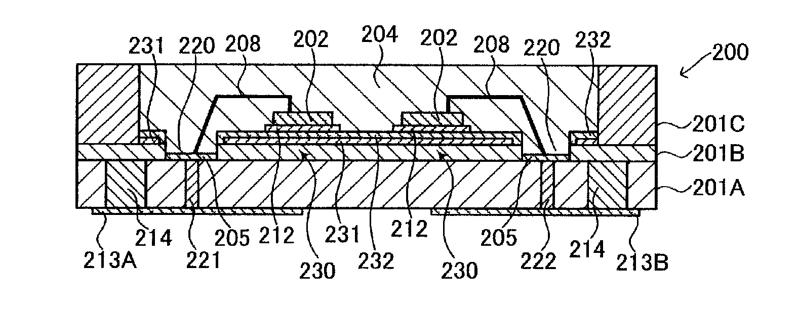
[0063]The structure of a semiconductor light emitting device according to a third embodiment will first be described with reference to FIGS. 6 to 9. FIG. 6A is a perspective view of the semiconductor light emitting device according to the third embodiment. FIG. 6B is a plan view of the semiconductor light emitting device. FIG. 7A is a bottom view of the semiconductor light emitting device. FIG. 7B is a schematic plan view for illustrating the positions of heat dissipation vias in the semiconductor light emitting device according to the third embodiment. FIG. 8A is a cross-sectional view taken along the line 8A-8A in FIG....


PUM

PropertyMeasurementUnit
thicknessaaaaaaaaaa
sizeaaaaaaaaaa
thicknessaaaaaaaaaa

Abstract

The device includes a first ceramic layer; a second ceramic layer on the first ceramic layer and having a light emitting element mounting area; a reflective layer so formed on a surface of the second ceramic layer that the reflective layer covers at least the mounting area; a protective layer which covers the reflective layer; a semiconductor light emitting element mounted on the protective layer positioned above the element mounting area; and at least one heat dissipation via passing through the first ceramic layer. The heat dissipation via is disposed in a position that does not overlap with the element mounting area in a direction in which the ceramic layers are stacked.

Description

BACKGROUND OF THE INVENTION[0001]1. Technical Field[0002]The present invention relates to a semiconductor light emitting device having a light emitting diode (LED) or any other semiconductor light emitting element mounted on a wiring substrate.[0003]2. Description of the Related Art[0004]A semiconductor light emitting device having an LED mounted on a wiring substrate has been used in an illuminator or lighting fixture, a backlight, an industrial apparatus, and other apparatus. In recent years, since the amount of heat generated in a semiconductor light emitting device itself increases as the intensity of the light from the semiconductor light emitting device increases, there is an increasing necessity to quickly dissipate the heat generated in the semiconductor light emitting device.[0005]To increase heat dissipation performance, there has been a known technique for forming a wiring substrate or wiring board on which an LED is mounted with a plurality of ceramic layers and providin...

Claims


Application Information

Patent Timeline
Patent Type & Authority Patents(United States)
IPC IPC(8): H01L33/00H01L31/12H01L29/267H01L27/15F21V29/00C03B29/00
CPCH01L33/486H01L33/60H01L25/167H01L33/647H01L2933/0033H01L2224/48091H01L2224/73265H01L2924/00014H01L2224/48095H01L2224/48228H01L2224/49175H01L2224/48227H01L2924/181H01L2924/00H01L2924/00012
Inventor TAKAYAMA, HIROYUKITANABE, MAIKONAMIOKA, KAORI
Owner STANLEY ELECTRIC CO LTD
Why Eureka
Try Eureka