Micro-scale power source

a power source and micro-scale technology, applied in the field of micro-scale power sources, can solve the problems of many electronic barriers broken, many size barriers broken, and significant obstacles in the power supply

Inactive Publication Date: 2013-10-08
UNIVERSITY OF MISSOURI
View PDF37 Cites 18 Cited by
  • Summary
  • Abstract
  • Description
  • Claims
  • Application Information

AI Technical Summary

Benefits of technology

[0008]In another embodiment, a micro-scale power source can include a semiconductor structure having a p-n junction formed of wide band-gap materials, and a radioisotope providing energy to the p-n junction. A radiation shield is located within the semiconductor structure. The radiation shield can comprise atoms implanted within a small volume of the semiconductor structure to form a micro bubble. The atoms defining the micro bubble can be selected from materials designed to locally change the band-gap properties of the semiconductor structure, and functions to assist with shielding the semiconductor structure from radiation damage.

Problems solved by technology

In countless modern devices, power supply remains a significant hurdle to further advancement and utility of the state of the art.
Many electronic barriers have been broken.
Many size barriers have been broken.
Self-contained and / or portable devices requiring energy for operation continue to be limited by a relatively lagging state of technological development of power sources.
In any number of devices ranging from detection equipment to laptop computers, the power source is primary limitation on continuous operation.
In many instances, the power supply also dwarfs the complicated electronics, displays, interfaces and other portions of a given device.
However, a fully miniaturized system requires a similarly miniaturized power source.

Method used


Image

  • Micro-scale power source
  • Micro-scale power source
  • Micro-scale power source

Examples


Embodiment Construction

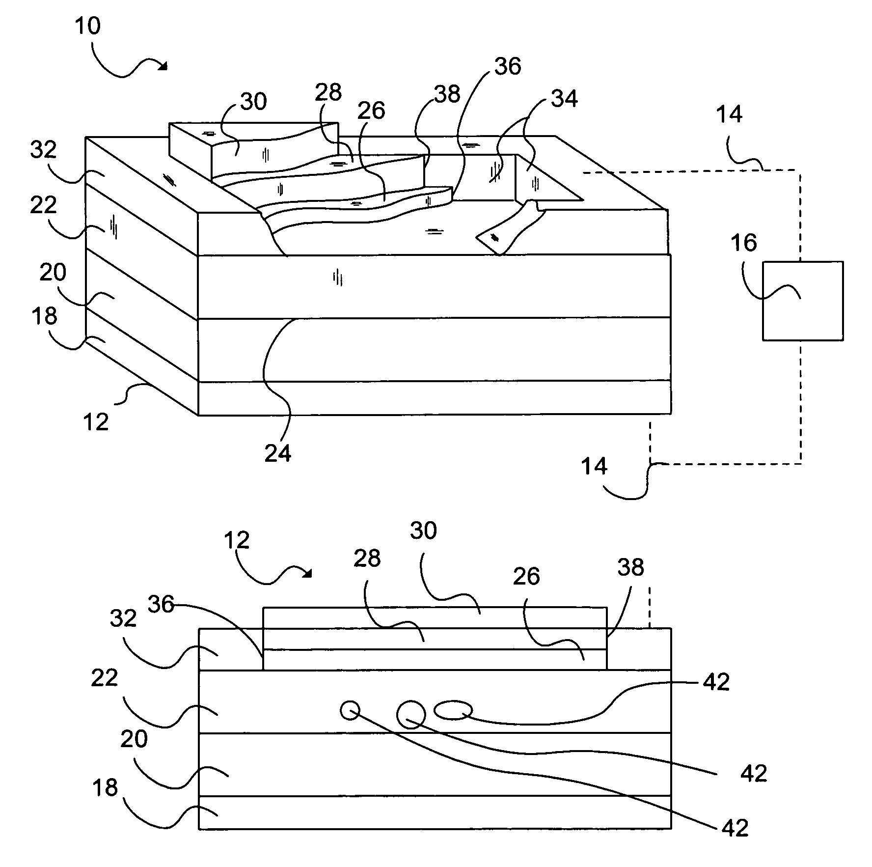
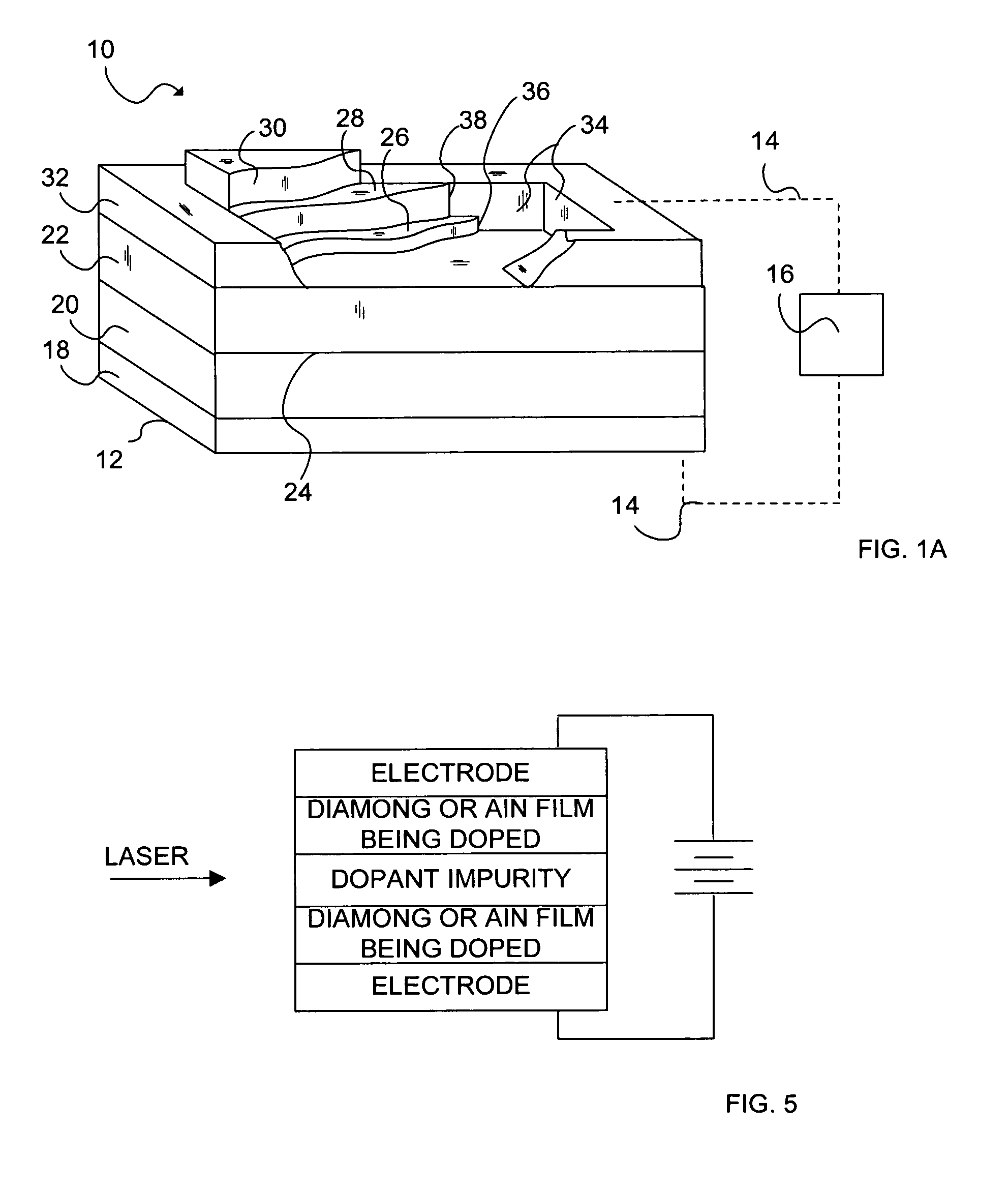
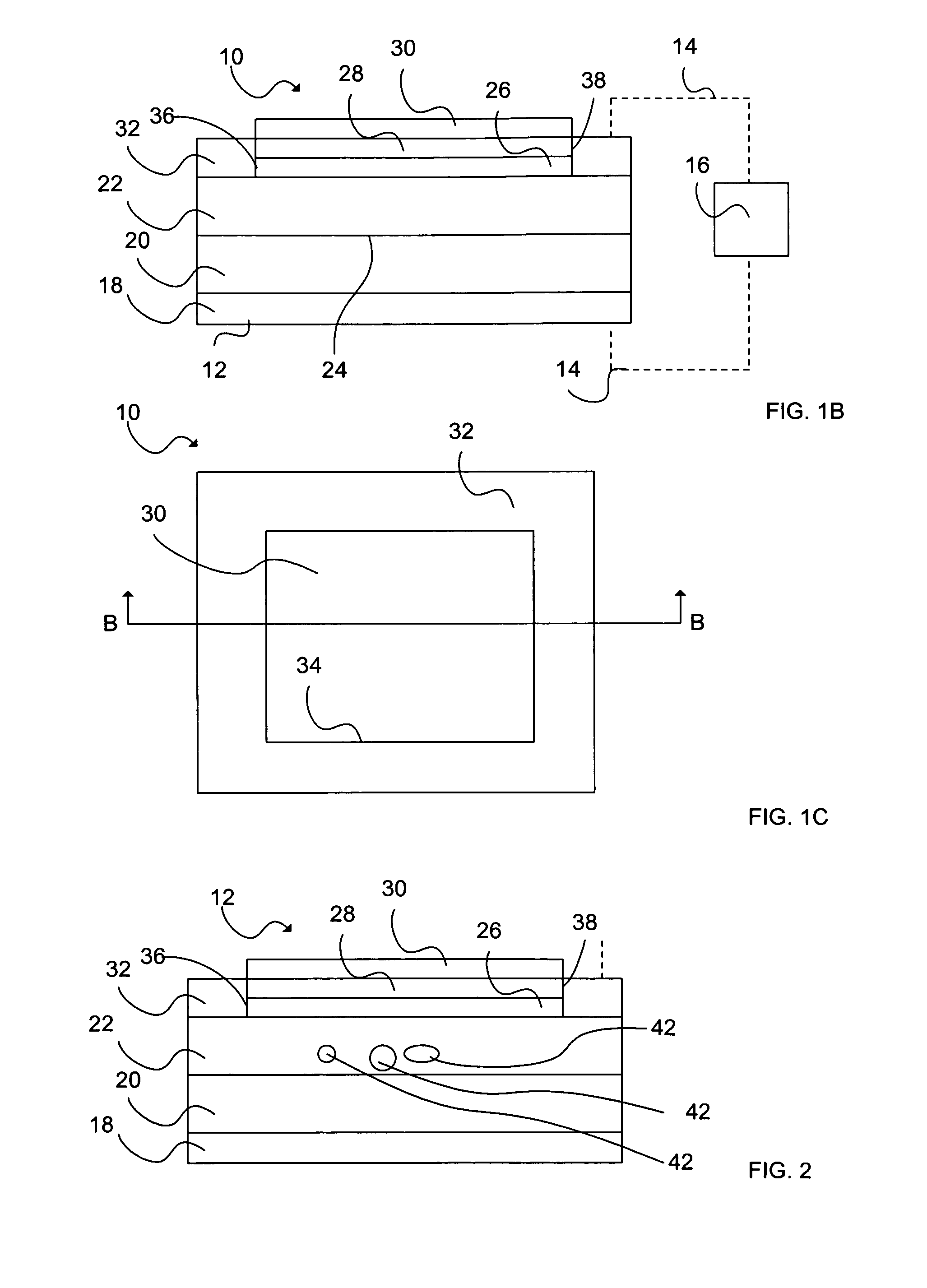
[0020]The invention is directed to a micro-scale power source. Embodiments of the invention may be integrated, for example, with MEMS. With such embodiments of the invention, a preferred formation process combines fabrication of the power source with that of the microelectromechanical structures. A self-powered MEMS device is formed.

[0021]The micro-scale power source of the invention makes use of wide band-gap materials in a semiconductor structure, such as a betavoltaic structure or cell. An embodiment of the invention is a betavoltaic device in which radioactive decay produces charge in a p-n junction formed of wide band-gap materials (See, e.g. FIG. 1A).

[0022]Radioisotope power conversion uses energy from the decay of radioisotopes to generate electrical power. Advantageously, radioisotope power can be used for applications that are considered inappropriate when using other power sources, such as generators, batteries, and solar cells. Some appropriate applications for using radi...


PUM


Abstract

A micro-scale power source and method includes a semiconductor structure having an n-type semiconductor region, a p-type semiconductor region and a p-n junction. A radioisotope provides energy to the p-n junction resulting in electron-hole pairs being formed in the n-type semiconductor region and p-type semiconductor region, which causes electrical current to pass through p-n junction and produce electrical power.

Description

PRIORITY CLAIM AND REFERENCE TO RELATED APPLICATION[0001]The present application claims the benefit of U.S. Provisional Patent Application No. 60 / 730,092, filed Oct. 25, 2005.FIELD OF THE INVENTION[0002]The field of the invention is power sources. Another field of the invention includes self-contained and / or portable devices requiring a power source. Particular exemplary applications of the invention include, for example, microelectromechanical systems (MEMS), portable electronics, military devices, and spacecraft.BACKGROUND ART[0003]In countless modern devices, power supply remains a significant hurdle to further advancement and utility of the state of the art. Many electronic barriers have been broken. Many size barriers have been broken. Self-contained and / or portable devices requiring energy for operation continue to be limited by a relatively lagging state of technological development of power sources. In any number of devices ranging from detection equipment to laptop computer...

Claims


Application Information

Patent Timeline
Patent Type & Authority Patents(United States)
IPC IPC(8): G21H1/06G21H1/00
CPCG21H1/06
Inventor PRELAS, MARK A.
Owner UNIVERSITY OF MISSOURI
Why Eureka
Try Eureka