Semiconductor light emitting device

a technology of semiconductor light and light emitting element, which is applied in the direction of discharge tube/lamp details, discharge tube luminescnet screen, lighting and heating apparatus, etc., can solve the problems of poor wavelength conversion efficiency, unresolved problems, and inefficient utilization of light output from semiconductor light emitting element as exciting light, etc., to achieve the effect of enhancing light extraction efficiency

Inactive Publication Date: 2013-10-15
STANLEY ELECTRIC CO LTD
View PDF16 Cites 14 Cited by
  • Summary
  • Abstract
  • Description
  • Claims
  • Application Information

AI Technical Summary

Benefits of technology

[0020]According to the present invention, light from the light emitting element is allowed to easily reach the first phosphor and the second phosphor, and the fluorescence being emitted is hardly absorbed by other phosphors, thereby enhancing light extraction efficiency.

Problems solved by technology

Therefore, there is a problem that the light outputted from the semiconductor light emitting element cannot be utilized efficiently as exciting light.
Therefore, the intensity of the ultraviolet radiation which reaches the blue phosphor is reduced, causing poor efficiency in wavelength conversion.
However, in here, the phosphor being used is just one type, and this does not solve the problem that exciting light or fluorescence is absorbed between multiple phosphors.
However, since the wavelengths of the fluorescence emitted from the respective cells are different from one another, there is a possibility that chromatic unevenness may occur in the in-plane direction.

Method used


Image

  • Semiconductor light emitting device
  • Semiconductor light emitting device
  • Semiconductor light emitting device

Examples


first embodiment

[0039]The light emitting device is a device for converting a part of blue light outputted from a blue light emitting flip-chip element, into red light and green light by using a color conversion plate, so as to emit white light which is obtained by mixing the blue, red, and green light.

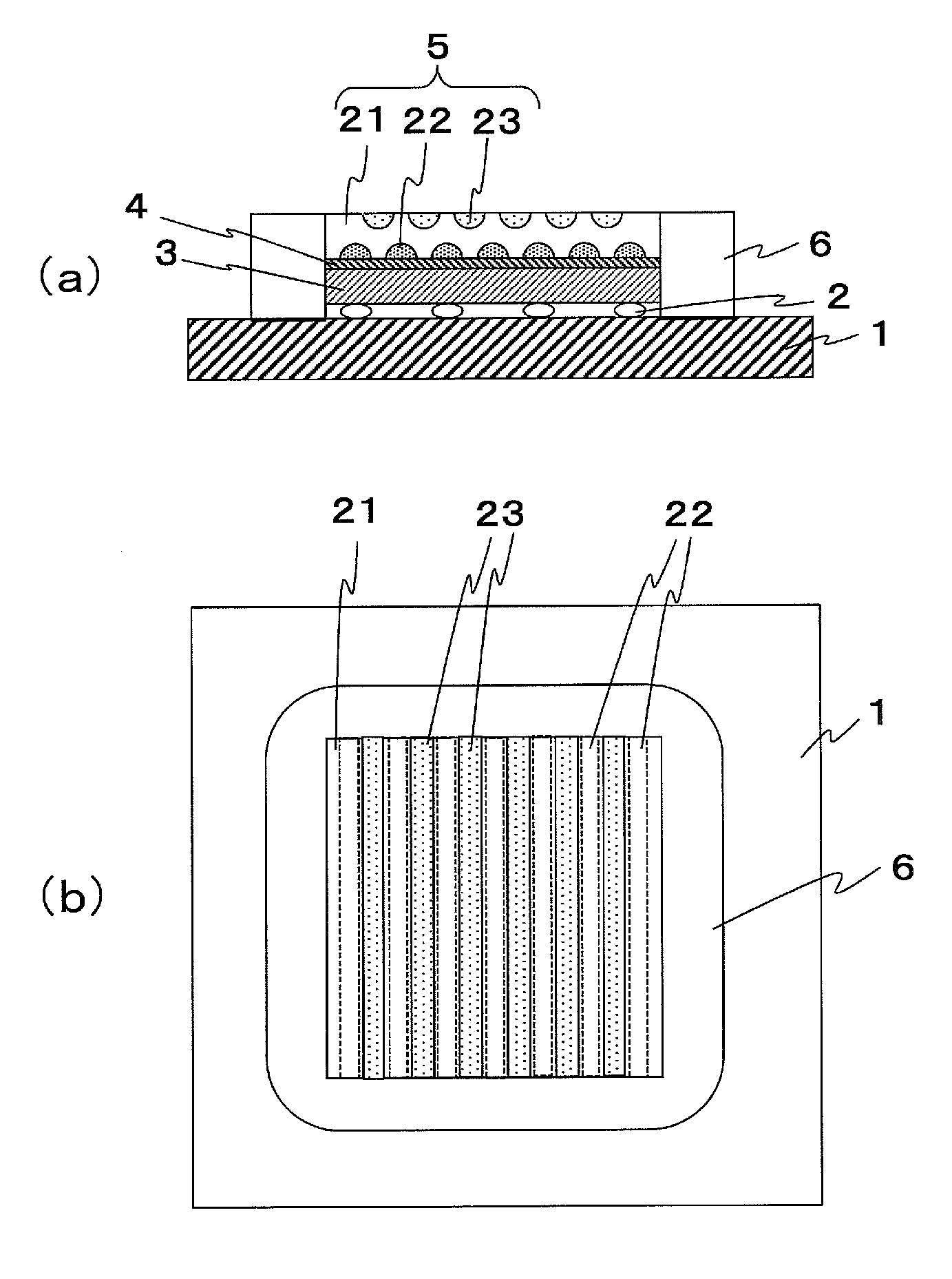
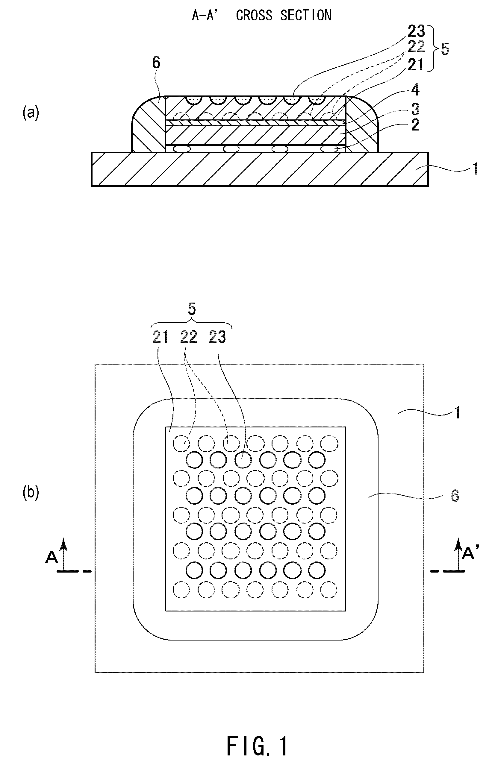
[0040]FIG. 1(a) illustrates a sectional view and FIG. 1(b) illustrates atop view of the light emitting device according to the first embodiment. As shown in FIG. 1(a), a flip-chip type semiconductor light emitting element 3 is implemented using Au bumps 2 on a substrate 1 on which electrode and wiring are formed in advance. On the semiconductor light emitting element 3, there is mounted a color conversion plate 5 via a transparent adhesion layer 4. Side surfaces of the semiconductor light emitting element 3 and the color conversion plate 5 are surrounded by an optical reflection frame 6.

[0041]The flip-chip type semiconductor light emitting element 3 includes, though not illustrated, an element substr...

second embodiment

[0067]The light emitting device will be explained with reference to FIG. 5(a) and FIG. 5(b). In the light emitting device as shown in FIG. 5(a) and FIG. 5(b), a semiconductor light emitting element 53 which emits blue light is implemented on the substrate 1 where electrode and wiring are formed in advance, by using AuSn eutectic 57 and Au bonding wire 56. The color conversion plate 5 is bonded on the semiconductor light emitting element 53 via the transparent adhesion layer 4.

[0068]The semiconductor light emitting element 53 includes an element substrate and a light emitting layer formed thereupon. The element substrate is a metal bonding (Metal Bonding: MB) element which is opaque to blue light. Hereinafter, in the present embodiment, the semiconductor light emitting element 53 is referred to as MB element 53. The MB element 53 is bonded to the substrate 1 by die bonding via AuSn eutectic 57, allowing the element substrate to face the substrate 1 and the light emitting layer to fa...

third embodiment

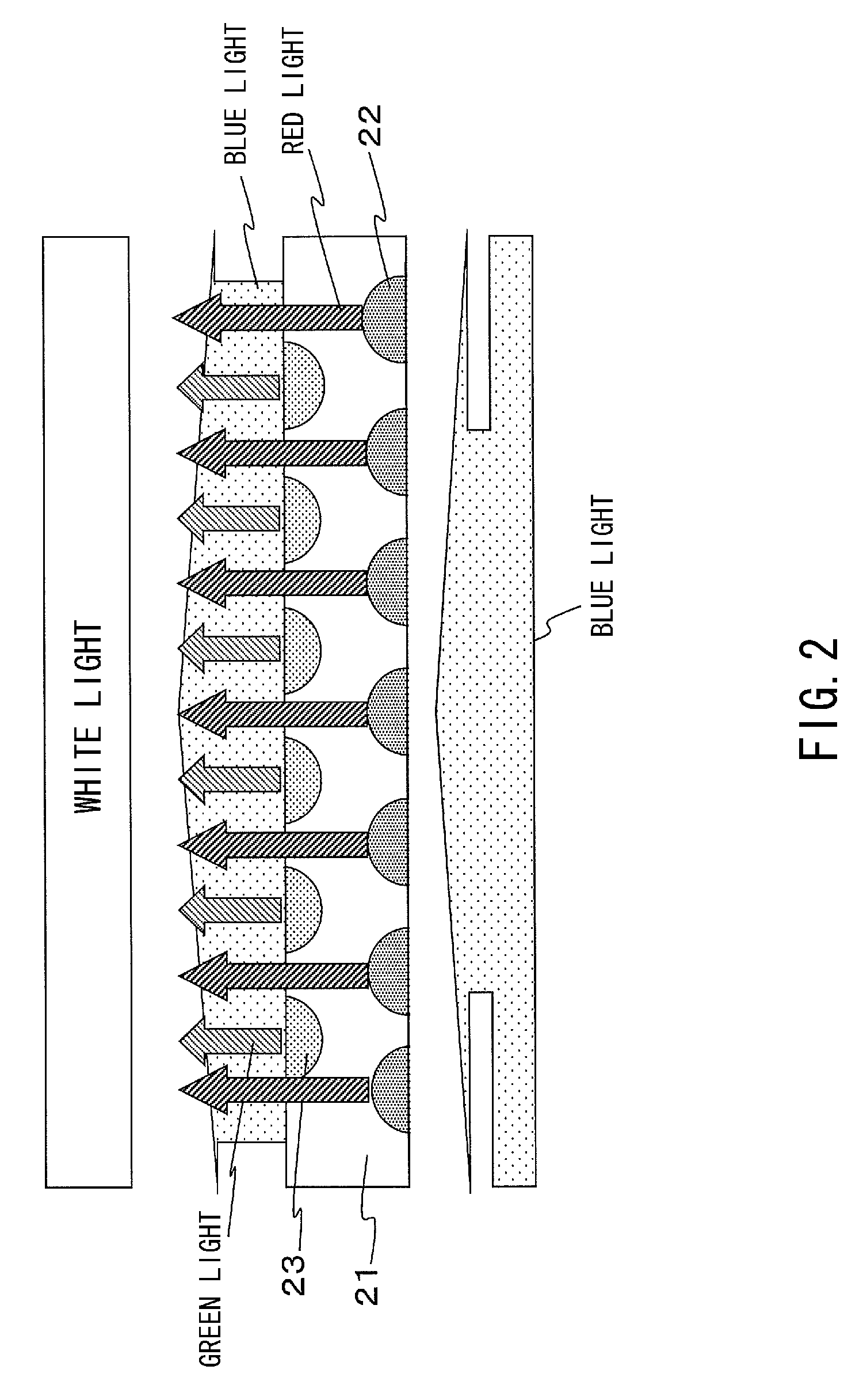
[0086]The blue light outputted from the light emitting element 3 passes through the color conversion plate 5, whereby a part of the blue light is converted into red fluorescence and green fluorescence as shown in FIG. 10. In addition, a part of the blue light directly passes through the transparent region 21, or transmits without absorbed by the red phosphor region 22 and the green phosphor region 23. By mixing those light elements, white light is obtained. Such operations as described above are the same as that of the

[0087]In the fifth embodiment, the stripe-like red phosphor regions 22 and green phosphor regions 23 are arranged in such a manner as orthogonal to each other, achieving a configuration that quadrangular transparent regions 21 are arranged vertically and horizontally at the positions where the spacing between the red phosphor regions 22 and the spacing between the green phosphor regions 23 superimpose one on another, when viewed from the top of the color conversion pla...


PUM


Abstract

A light emitting device can make it hard for fluorescence emitted from each phosphor in a color conversion plate to be absorbed by other phosphor. The color conversion plate can include multiple types of phosphors, and the light from a light emitting element can be allowed to reach each of the phosphors efficiently. The color conversion plate can contain at least first and second phosphors which absorb light emitted from the light emitting element and outputs fluorescence. The color conversion plate can have multiple first regions containing the first phosphor on a light emitting element side, being arranged with a predetermined spacing therebetween, and second regions containing the second phosphor on the upper surface, being arranged with a predetermined spacing therebetween. A region where the first regions and the second regions are excluded, as viewed from a location on top of the conversion plate, contains no phosphor.

Description

[0001]This application claims the priority benefit under 35 U.S.C. §119 of Japanese Patent Application No. 2010-176545 filed on Aug. 5, 2010, which is hereby incorporated in its entirety by reference.FIELD OF THE INVENTION[0002]The present invention relates to a semiconductor light emitting device provided with a member which subjects an outgoing beam from a semiconductor light emitting element to wavelength conversion.DESCRIPTION OF THE RELATED ART[0003]There is known a light emitting element which is formed by arranging two or more types of phosphor layers on the semiconductor light emitting element, and converts the light from the semiconductor light emitting element into light having two or more wavelengths, thereby outputting light which is generated by mixing these various types of light.[0004]By way of example, Japanese Unexamined Patent Application Publication No. 2004-179644 (hereinafter referred to as “patent document 1”) and Japanese Unexamined Patent Application Publicat...

Claims


Application Information

Patent Timeline
Patent Type & Authority Patents(United States)
IPC IPC(8): H01J1/62H01J63/04
CPCH01L33/504H01L33/505H01L33/508H01L2933/0041H01L2224/73265H01L2224/48091H01L2224/45144H01L2924/3025H01L2924/00014H01L2924/00
Inventor HARADA, MITSUNORI
Owner STANLEY ELECTRIC CO LTD
Why Eureka
Try Eureka