Semiconductor device and manufacturing method thereof

a technology of semiconductor devices and manufacturing methods, applied in the direction of semiconductor devices, basic electric elements, electrical appliances, etc., can solve the problems of power consumption suppression, so-called aperture ratio reduction, etc., and achieve the effect of small loss of current, small off current, and high reliability

Active Publication Date: 2013-10-22
SEMICON ENERGY LAB CO LTD
View PDF174 Cites 7 Cited by
  • Summary
  • Abstract
  • Description
  • Claims
  • Application Information

AI Technical Summary

Benefits of technology

[0023]Therefore, an object of the present invention is to provide a transistor having both a light-transmitting property and so-called normally-off characteristics. Another object of the present invention is to provide a transistor having both a light-transmitting property and a characteristic of smaller off current. Another object of the present invention is to provide a transistor having both a light-transmitting property and a characteristic of small loss of on current. Another object of the present invention is to provide a transistor where change in property over time is suppressed.
[0025]To provide a light-transmitting transistor, a gate electrode, a source electrode, and a drain electrode are needed to be formed using a light-transmitting conductive film. To reduce the loss of on current of a transistor, it is necessary to increase conductivities of a source electrode and a drain electrode. Thus, in the case where a source electrode and a drain electrode of a transistor are formed using a light-transmitting conductive layer, an oxide conductive layer is favorably used. In particular, an oxide conductive layer containing oxygen vacancy and an impurity (such as hydrogen) which increase conductivity is favorable because it has high conductivity.
[0026]To provide a light-transmitting transistor, a semiconductor layer including a channel formation region needs to have a light-transmitting property. To reduce power consumption of a transistor, an operating characteristic of normally off and a characteristic of sufficiently small off current are necessary. Therefore, an oxide semiconductor layer having a lower carrier concentration and a wide band gap is suitable to a semiconductor layer including a channel formation region.
[0030]To achieve the above objective, movement of hydrogen and oxygen may be suppressed in a region where the oxide conductive layer for forming a source electrode and a drain electrode is electrically connected to the oxide semiconductor layer.
[0031]Specifically, a structure may be adopted in which an oxide semiconductor having a wide band gap and a carrier concentration which is as low as possible is used as the oxide semiconductor layer including a channel formation region, an oxide conductor containing hydrogen and oxygen vacancy is used for the source electrode and the drain electrode, a barrier layer which prevents diffusion of hydrogen and oxygen between the oxide conductive layer and the oxide semiconductor layer is provided, and the oxide conductive layer and the oxide semiconductor layer are electrically connected to each other through the barrier layer.
[0046]A transistor having a light-transmitting property and normally-off characteristics can be provided. A transistor having a light-transmitting property and a characteristic of smaller off current can be provided. A transistor having a light-transmitting property and a characteristic of small loss of on current can be provided. The light-transmitting transistor with high reliability, in which change in property over time is suppressed, can be provided.

Problems solved by technology

In an active matrix semiconductor device in which pixels each provided with a transistor are arranged in matrix, as the pixel is miniaturized, the proportion of the area of the transistor in the pixel is increased; thus, there occurs a problem of reduction in so-called aperture ratio.
In addition, a problem of energy depletion in recent years has caused a demand for a display device whose power consumption is suppressed.

Method used


Image

  • Semiconductor device and manufacturing method thereof
  • Semiconductor device and manufacturing method thereof
  • Semiconductor device and manufacturing method thereof

Examples


embodiment 1

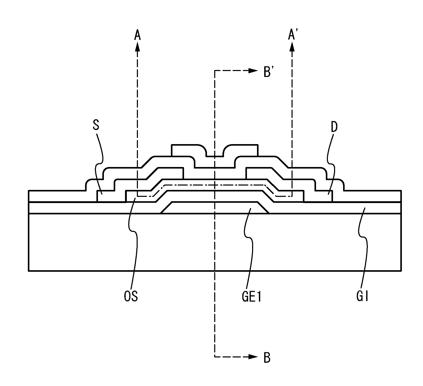
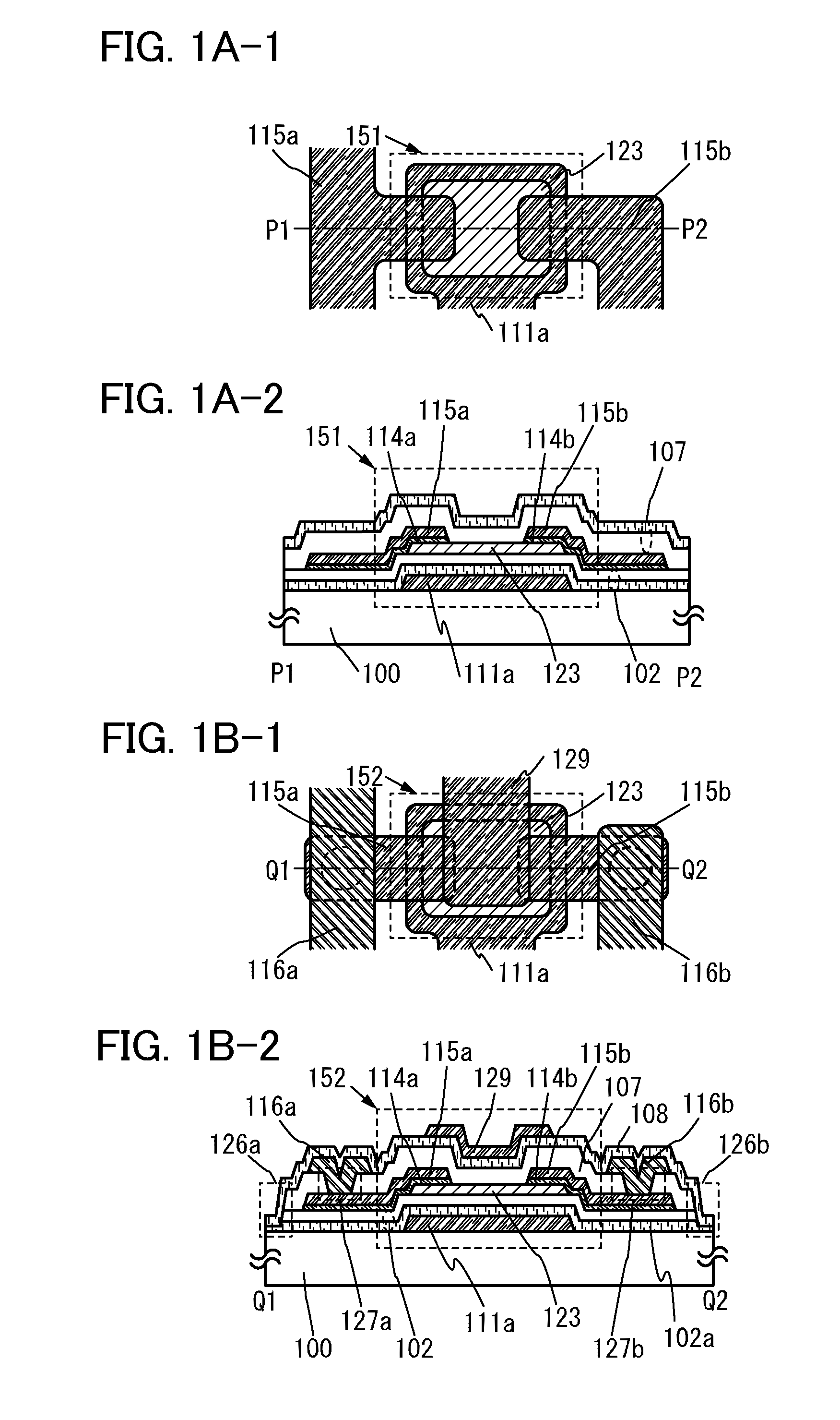
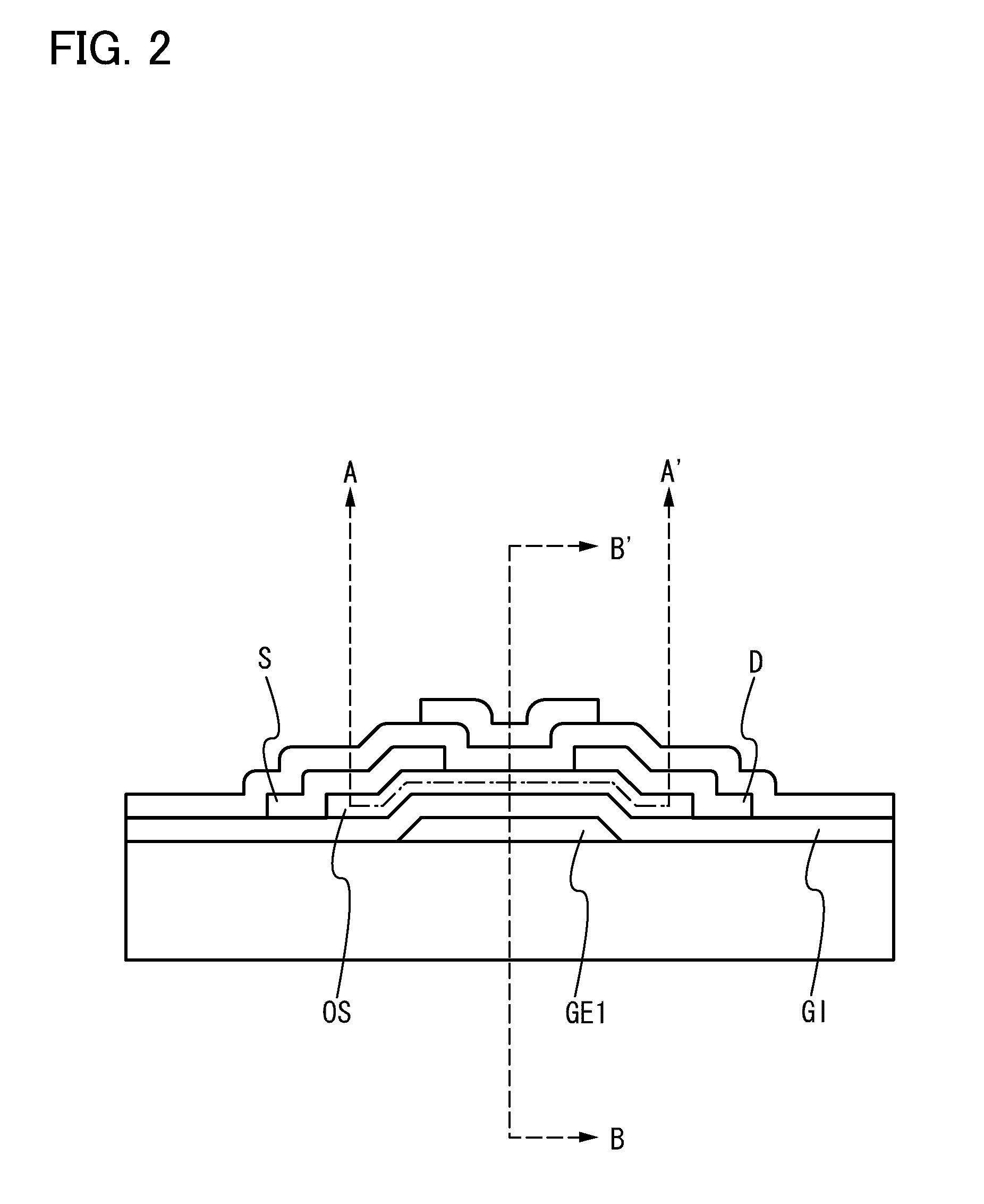
[0072]In this embodiment, a bottom-gate transistor which transmits visible light will be described as an embodiment of a semiconductor device with reference to FIGS. 1A-1, 1A-2, 1B-1, and 1B-2.

[0073]FIGS. 1A-1 and 1A-2 illustrate an example in which an electrode of a transistor and a wiring connected to the transistor are formed using light-transmitting conductive films.

[0074]FIGS. 1B-1 and 1B-2 illustrate an example in which an electrode of a transistor is formed using a light-transmitting conductive film and a wiring connected to the transistor is formed using a conductive film containing metal.

[0075]FIGS. 1A-1 and 1A-2 illustrate an embodiment of a structure of a bottom-gate transistor which transmits visible light. FIG. 1A-1 is a top plan view illustrating a plane structure of the transistor, and FIG. 1A-2 is a cross-sectional view illustrating a layered structure of the transistor. Note that a dashed-dotted line P1-P2 in FIG. 1A-1 corresponds to a cross section P1-P2 in FIG. 1A...

embodiment 2

[0141]In this embodiment, a display device for which a bottom-gate transistor which transmits visible light is used will be described as an embodiment of a semiconductor device with reference to FIGS. 6A and 6B. In addition, a method for manufacturing the bottom-gate transistor which transmits visible light will be described with reference to FIGS. 7A to 7D.

[0142]A method for manufacturing a channel-protective transistor which can be formed together with the bottom-gate transistor which transmits visible light will also be described with reference to FIGS. 7A to 7D.

[0143]FIG. 6A is a top plan view illustrating a pixel portion of a display device for which a bottom-gate transistor which transmits visible light is used. FIG. 6B is a cross-sectional view illustrating a layered structure of the pixel portion of the display device for which a bottom-gate transistor which transmits visible light is used. Note that a dashed-dotted line A1-A2 in FIG. 6A corresponds to a cross section A1-A2 ...

embodiment 3

[0236]In this embodiment, an example of a structure of a terminal portion provided over a substrate over which a semiconductor device is provided is illustrated in FIGS. 8A-1, 8A-2, 8B-1, and 8B-2. Note that in FIGS. 8A-1, 8A-2, 8B-1, and 8B-2, the portions which are the same as those in FIGS. 1A-1, 1A-2, 1B-1, and 1B-2 are denoted by common reference numerals.

[0237]FIGS. 8A-1 and 8A-2 illustrate a top plan view and a cross-sectional view of a terminal portion of a gate wiring, respectively. FIG. 8A-1 corresponds to a cross-sectional view along j-k in FIG. 8A-2.

[0238]In FIG. 8A-1, a first terminal 411 is a connection terminal functioning as an input terminal. As for the first terminal 411, a conductive layer 111e formed of the same material as the gate wiring and a conductive layer 115e formed of the same material as a second conductive layer are stacked with a barrier layer 114e therebetween. Although not illustrated in the drawing, the conductive layer 111e is electrically connect...


PUM


Abstract

A semiconductor device includes an oxide semiconductor layer including a channel formation region which includes an oxide semiconductor having a wide band gap and a carrier concentration which is as low as possible, and a source electrode and a drain electrode which include an oxide conductor containing hydrogen and oxygen vacancy, and a barrier layer which prevents diffusion of hydrogen and oxygen between an oxide conductive layer and the oxide semiconductor layer. The oxide conductive layer and the oxide semiconductor layer are electrically connected to each other through the barrier layer.

Description

TECHNICAL FIELD[0001]The present invention relates to a semiconductor device including a semiconductor element and a method for manufacturing the semiconductor device.[0002]Note that a semiconductor device in this specification indicates all the devices that can operate by using semiconductor characteristics, and semiconductor elements such as transistors; and electro-optical devices, semiconductor circuits, and electronic appliances which include semiconductor elements are all semiconductor devices.BACKGROUND ART[0003]A technique by which transistors are manufactured using oxide semiconductors for channel formation regions and the transistors are applied to semiconductor circuits, ICs, electro-optical devices, electronic appliances, and the like has attracted attention.[0004]In particular, an oxide semiconductor having a wide band gap transmits visible light; therefore, the following is attempted: a light-transmitting transistor is manufactured using such an oxide semiconductor wit...

Claims


Application Information

Patent Timeline
Patent Type & Authority Patents(United States)
IPC IPC(8): H01L29/04H01L31/0376H01L31/036H01L31/20
CPCH01L27/1225H01L29/45H01L29/66742H01L29/7869H10K50/828
Inventor YAMAZAKI, SHUNPEIAKIMOTO, KENGO
Owner SEMICON ENERGY LAB CO LTD
Why Eureka
Try Eureka