Layout method for soft-error hard electronics, and radiation hardened logic cell
What is AI technical title?
AI technical title is built by Patsnap AI team. It summarizes the technical point description of the patent document.
a logic cell and hard electronics technology, applied in the field of soft-error hard electronics and radiation-hardened logic cells, can solve problems such as voltage pulses in circuits, and achieve the effect of reducing the effect of single event and protecting against soft errors
Active Publication Date: 2013-10-22
LILJA KLAS OLOF
View PDF54 Cites 14 Cited by
Summary
Abstract
Description
Claims
Application Information
AI Technical Summary
This helps you quickly interpret patents by identifying the three key elements:
Problems solved by technology
Method used
Benefits of technology
Benefits of technology
This patent describes a new way to design circuits that can protect against errors caused by single events. The method takes advantage of the way that multiple parts of the circuit can interact to cancel out the effects of a single event. The layout of the circuit also includes special cells that are designed to prevent errors caused by soft errors. This method ensures that the combination of multiple circuits is always error-free, which is important for maintaining the accuracy of signals in the circuit.
Problems solved by technology
This leads to current pulses on the circuit nets, connected to these contact areas, which, in their turn, cause voltage pulses in the circuit which can upset a sequential element (latch, flip-flop) or propagate through combinational logic and be latched in as errors at the next sequential element in the circuit.
Method used
Image
Click on the blue label to locate the original text in one second.
Reading with bidirectional positioning of images and text.
Examples
Embodiment Construction
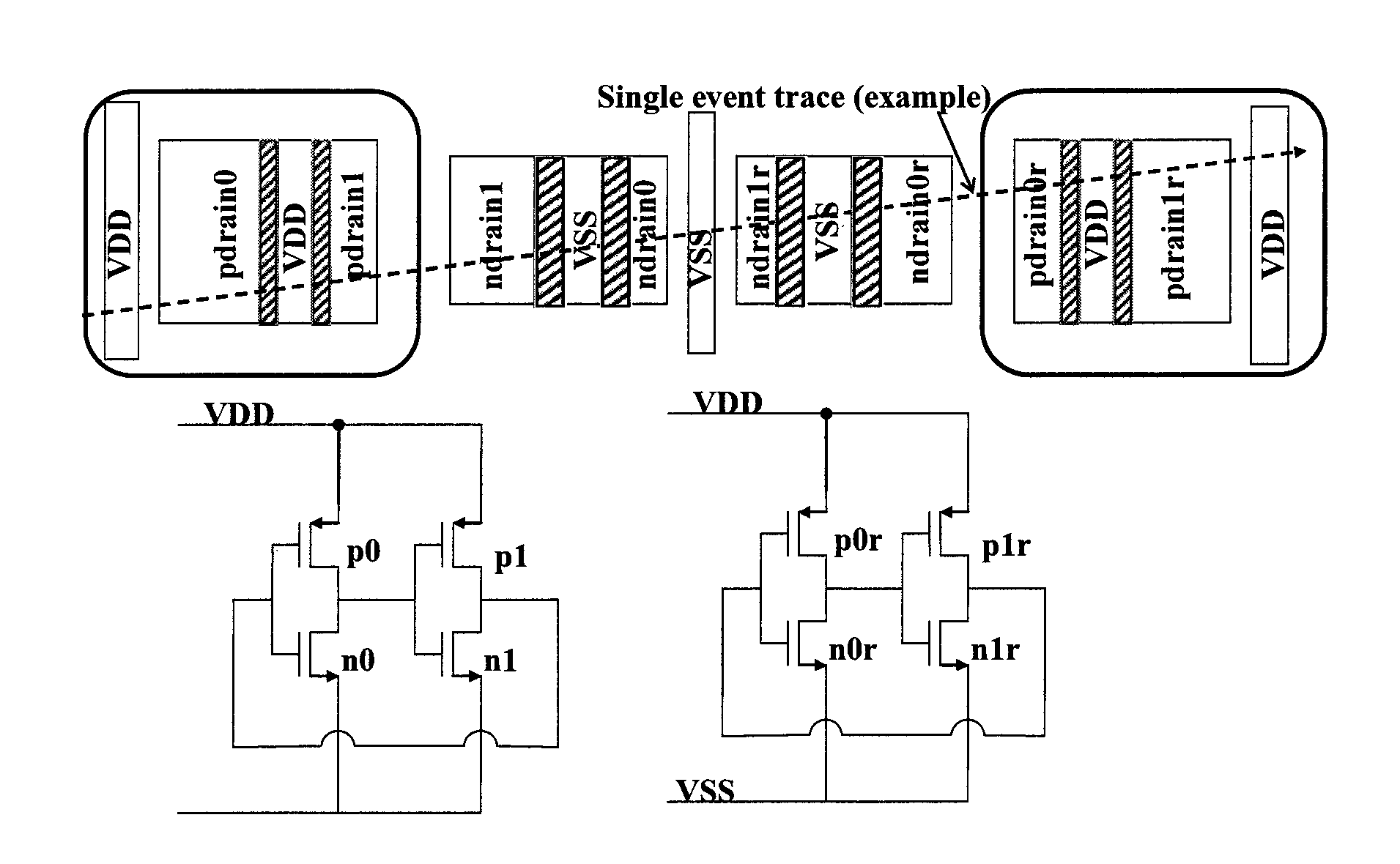
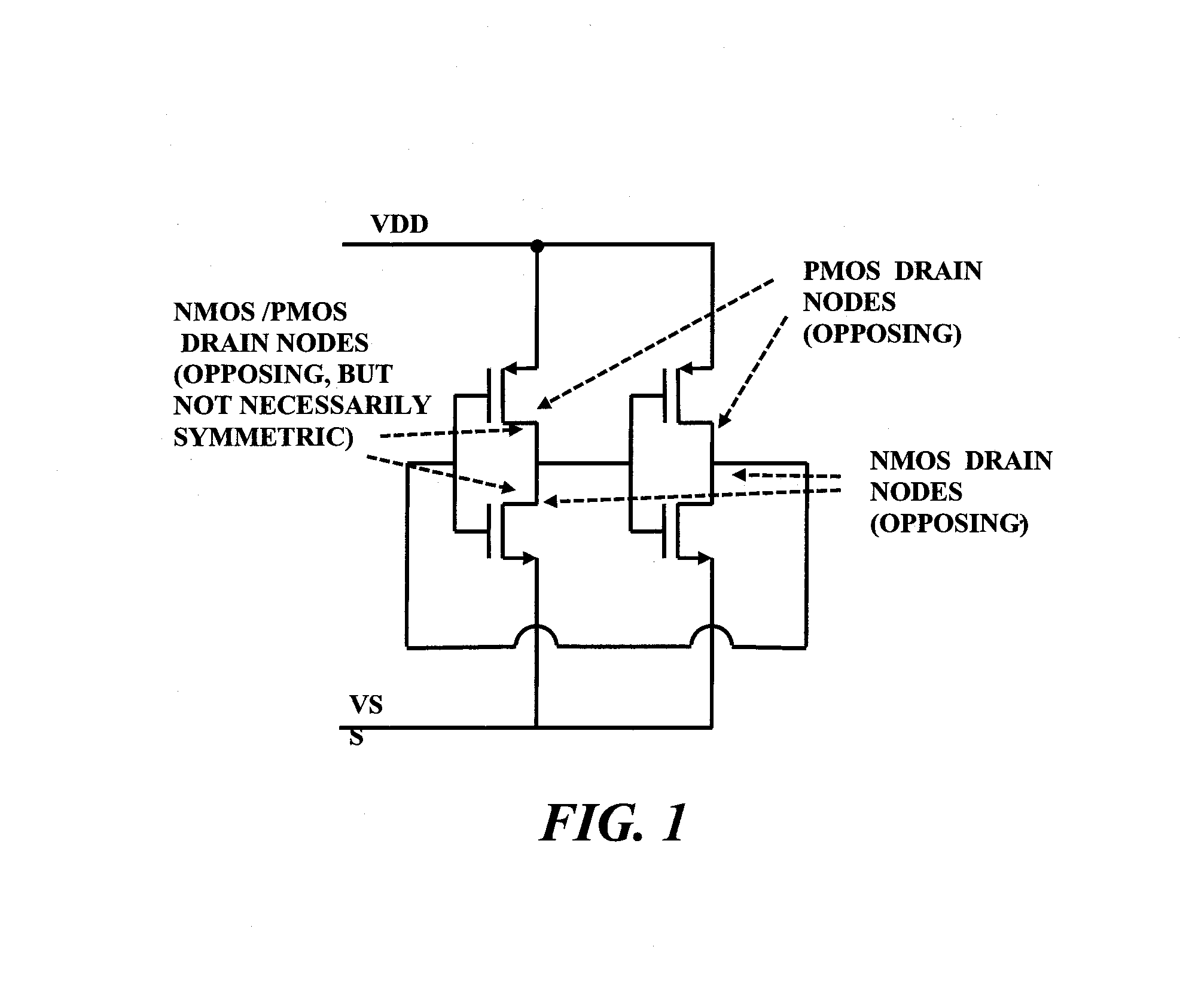
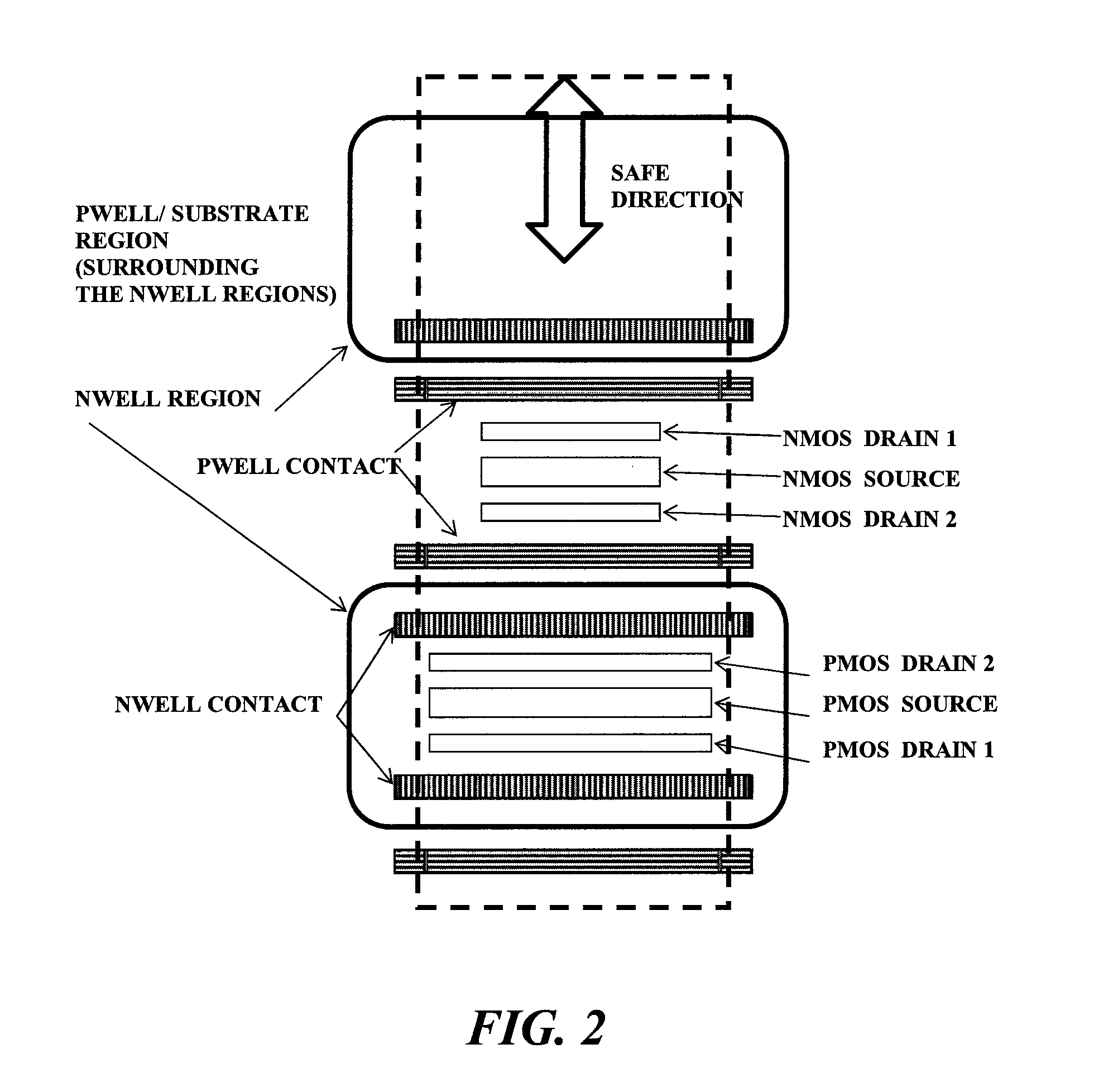
[0029]This invention comprises a unique new layout method, which takes advantage of the overall circuit response to a single event effect. It also includes specific circuit cells with layout, which have been constructed in accordance with the new layout method.
[0030]A radiation generated single event (soft-) error (SEE) occurs when the charge, generated in the semiconductor material by one or more (e.g. secondary) charged particles, is collected by contact areas. The contact areas are the low resistivity regions on, or in, the semiconductor substrate, which are connected to a net in the circuit, e.g., the source and drain areas in a MOSFET technology. A circuit net (or node) refers to a part of the circuit, connected by low resistivity regions (metal), which maintains a certain voltage value (referred to as the voltage state of the net) throughout its' extent. A net can be connected to any number of contact areas.
[0031]The charge collected by contact areas during a single event, lea...
PUM
Abstract
This invention comprises a layout method to effectively protect logic circuits against soft errors (non-destructive errors) and circuit cells, with layout, which are protected against soft errors. In particular, the method protects against cases where multiple nodes in circuit are affected by a single event. These events lead to multiple errors in the circuit, and while several methods exist to deal with single node errors, multiple node errors are very hard to deal with using any currently existing protection methods. The method is particularly useful for CMOS based logic circuits in modern technologies (.ltoreq.90 nm), where the occurrence of multiple node pulses becomes high (due to the high integration level). It uses a unique layout configuration, which makes the circuits protected against single event generated soft-errors.
Description
CROSS REFERENCE TO RELATED APPLICATIONS[0001]This application is a divisional application, claiming the priority of U.S. application Ser. No. 12 / 354,655, Entitled: “Layout Method for Soft-Error Hard Electronics, and Radiation Hardened Logic Cell”, filed Jan. 15, 2009, also claiming priority to U.S. application No. 61 / 011,599, Entitled: “Layout Methodology for Soft-Error Hard Electronics”, filed Jan. 17, 2008, also claiming priority to U.S. provisional application No. 61 / 011,989, Entitled: “Robust Cell Layout Synthesis Methodology for Soft-Error Hard Electronics”, filed Jan. 22, 2008, also claiming priority to U.S. provisional application No. 61 / 068,483, Entitled: “Circuit and Layout for a Radiation Hard Sequential Circuit Element”, filed Mar. 7, 2008, also claiming priority to U.S. provisional application No. 61 / 123,003, Entitled: “Design Technique, and Layout and Circuit Configurations, for Radiation Hardening of Logic Circuits”, filed Apr. 5, 2008, which are incorporated herein by...
Claims
Application Information
Patent Timeline
Application Date:The date an application was filed.
Publication Date:The date a patent or application was officially published.
First Publication Date:The earliest publication date of a patent with the same application number.
Issue Date:Publication date of the patent grant document.
PCT Entry Date:The Entry date of PCT National Phase.
Estimated Expiry Date:The statutory expiry date of a patent right according to the Patent Law, and it is the longest term of protection that the patent right can achieve without the termination of the patent right due to other reasons(Term extension factor has been taken into account ).
Invalid Date:Actual expiry date is based on effective date or publication date of legal transaction data of invalid patent.

