Semiconductor light-emitting element, electrode and manufacturing method for the element, and lamp

a technology of semiconductor light-emitting elements and manufacturing methods, which is applied in the manufacturing of semiconductor/solid-state devices, semiconductor devices, electrical equipment, etc., can solve the problems of not being able to extract a portion of the emitted light out of the light-emitting element, the bonding pad electrode is unable to resist the tensile stress, and the electrode itself is difficult to use as a bonding pad electrode, etc., to prevent the light from being peeled off, the junction and anticorrosion properties

Active Publication Date: 2013-10-29
TOYODA GOSEI CO LTD
View PDF25 Cites 9 Cited by
  • Summary
  • Abstract
  • Description
  • Claims
  • Application Information

AI Technical Summary

Benefits of technology

[0063]According to the above-described configuration of the present invention, a semiconductor light-emitting element having an electrode with improved junction and anticorrosion properties, a manufacturing method therefor, and a lamp can be provided.
[0064]According to a semiconductor light-emitting element according to the present invention, one electrode is composed of a junction layer and a bonding pad electrode formed to cover the junction layer, the bonding pad electrode has a maximum thickness that is larger than the maximum thickness of the junction layer and is composed of one or two or more layers, and slopes, which are made gradually thinner toward the outer circumference, are formed in outer circumference portions of the junction layer and the bonding pad electrode. Accordingly, penetration of external air or moisture into the junction layer can be prevented, and thus the anticorrosion property of the junction layer can be improved to lengthen the life span of the semiconductor light-emitting element.
[0065]According to the semiconductor light-emitting element according to the present invention, the junction layer is made of at least one kind of element selected from the group consisting of Al, Ti, V, Cr, Mn, Co, Zn, Ge, Zr, Nb, Mo, Ru, Hf, Ta, W, Re, Rh, Ir, and Ni, and is a thin film of which the maximum thickness is equal to or more than 10 Å and equal to or less than 1000 Å. Accordingly, the junction between the transparent electrode and the bonding pad electrode is improved, and thus the electrode is prevented from being peeled off due to the tensile stress occurring during the bonding of the bonding wire.
[0066]According to the semiconductor light-emitting element according to the present invention, the bonding pad electrode is composed of a bonding layer made of Au, Al, or an alloy including any one of these metals, and the bonding layer is a thin film of which the maximum thickness is equal to or more than 50 nm and equal to or less than 2000 nm. Accordingly, the junction of the wire bonding to the bonding pad electrode is improved, and thus the electrode is prevented from being peeled off due to the tensile stress occurring during the bonding of the bonding wire.
[0067]According to the semiconductor light-emitting element according to the present invention, the bonding pad electrode is composed of a metal reflection layer formed to cover the junction layer and a bonding layer formed to cover the metal reflection layer, and the metal reflection layer 117 is made of any one of Ag, Al, Ru, Rh, Pd, Os, Ir, Pt, and Ti or an alloy including any one of these metals, and is a thin film of which the maximum thickness is equal to or more than 20 nm and equal to or less than 3000 nm. Accordingly, the junction and anticorrosion properties of the electrode are improved, and thus the light-emitting characteristics of the semiconductor light-emitting element can be improved.
[0068]According to an electrode for a semiconductor light-emitting element according to the present invention, at least one of the one electrode and the other electrode is composed of a junction layer and a bonding pad electrode formed to cover the junction layer, the bonding pad electrode has a maximum thickness that is larger than the maximum thickness of the junction layer and is composed of one or two or more layers, and slopes, which are made gradually thinner toward the outer circumference, are formed in outer circumference portions of the junction layer and the bonding pad electrode. Accordingly, the electrode has improved junction and anticorrosion properties. The electrode for a semiconductor light-emitting element according to the present invention can also be used for the intended purpose in addition to the light-emitting element.

Problems solved by technology

However, the transparent electrode composed of metal oxide such as ITO or the ohmic electrode composed of a metal thin film of about several tens of nanometers has as low a strength as the electrode itself, and thus it is difficult to use the electrode itself as a bonding pad electrode.
However, since this bonding pad electrode is a metal material having a specified thickness, it has no transparency and shields the emitted light that has transmitted the p-type electrode having transparency.
As a result, there is a problem that it may not be possible to extract a portion of the emitted light out of the light-emitting element.
However, if it is intended to bond a bonding wire or the like with the bonding pad electrode in the case where the metal oxide such as ITO is used as the p-type electrode and the reflection film such as Ag, Al, is used as the bonding pad electrode, the bonding pad electrode is unable to resist the tensile stress during bonding of the bonding wire, and thus the pad electrode may be peeled off.
Also, as the bonding pad electrode is peeled off from the transparent electrode, the yield in manufacturing a lamp that uses such electrodes may deteriorate.
Also, in the semiconductor light-emitting element in the related art, the anticorrosion property is insufficient, and thus there is a demand for improvement of the anticorrosion property.

Method used


Image

  • Semiconductor light-emitting element, electrode and manufacturing method for the element, and lamp
  • Semiconductor light-emitting element, electrode and manufacturing method for the element, and lamp
  • Semiconductor light-emitting element, electrode and manufacturing method for the element, and lamp

Examples


embodiment 1

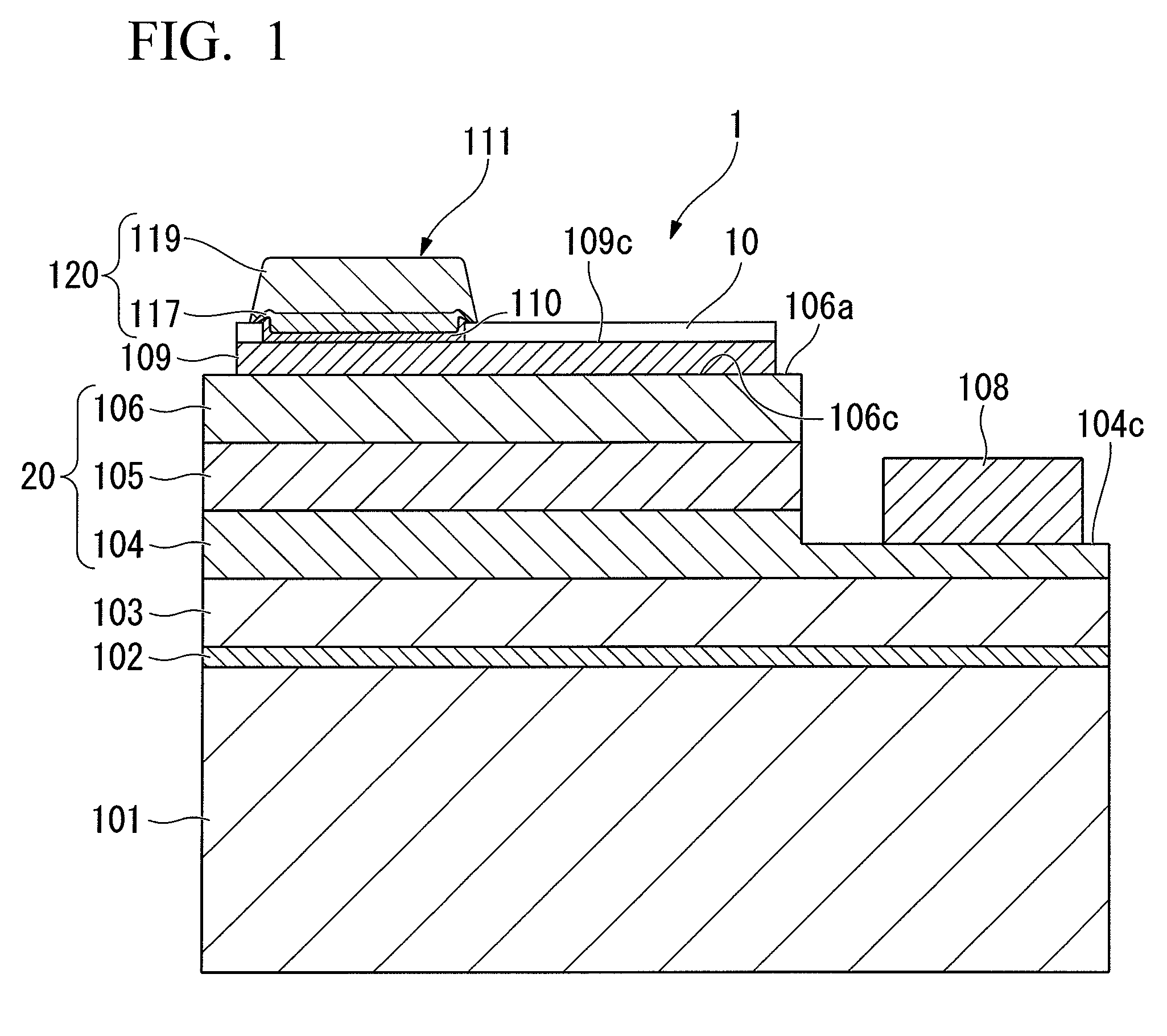
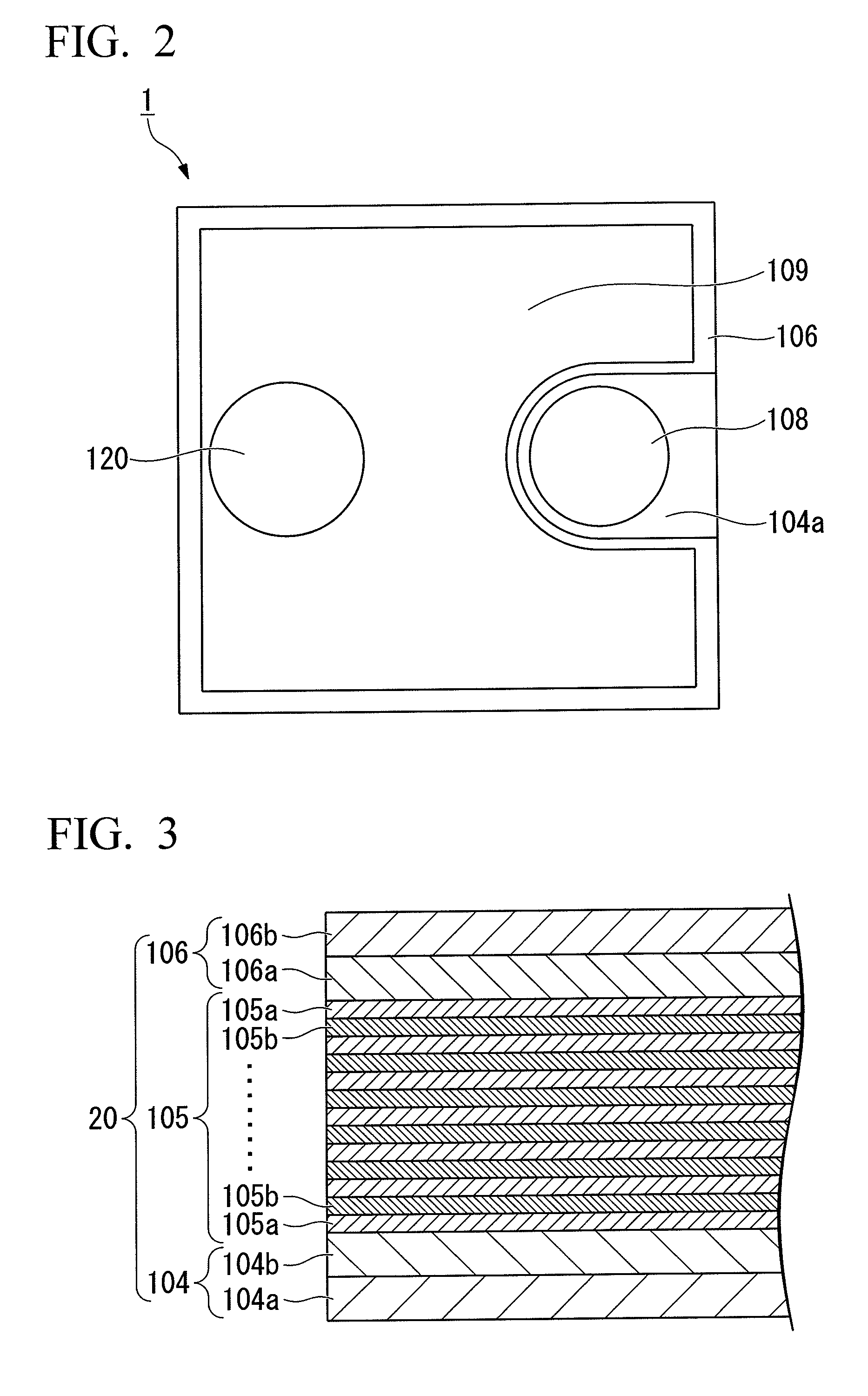
[0116]FIGS. 1 to 4 are views illustrating an example of a semiconductor light-emitting element according to an embodiment of the present invention. FIG. 1 is a schematic cross-sectional view illustrating an example of a semiconductor light-emitting element according to an embodiment of the present invention, and FIG. 2 is a schematic plan view illustrating an example of a semiconductor light-emitting element according to an embodiment of the present invention. FIG. 3 is a schematic cross-sectional view illustrating an example of a laminated semiconductor layer of a semiconductor light-emitting element according to an embodiment of the present invention, and FIG. 4 is an example of an enlarged cross-sectional view of a p-type electrode of a semiconductor light-emitting element according to an embodiment of the present invention.

[0117](Semiconductor Light-Emitting Element)

[0118]As illustrated in FIG. 1, a semiconductor light-emitting element 1 according to an embodiment of the present...

embodiment 7

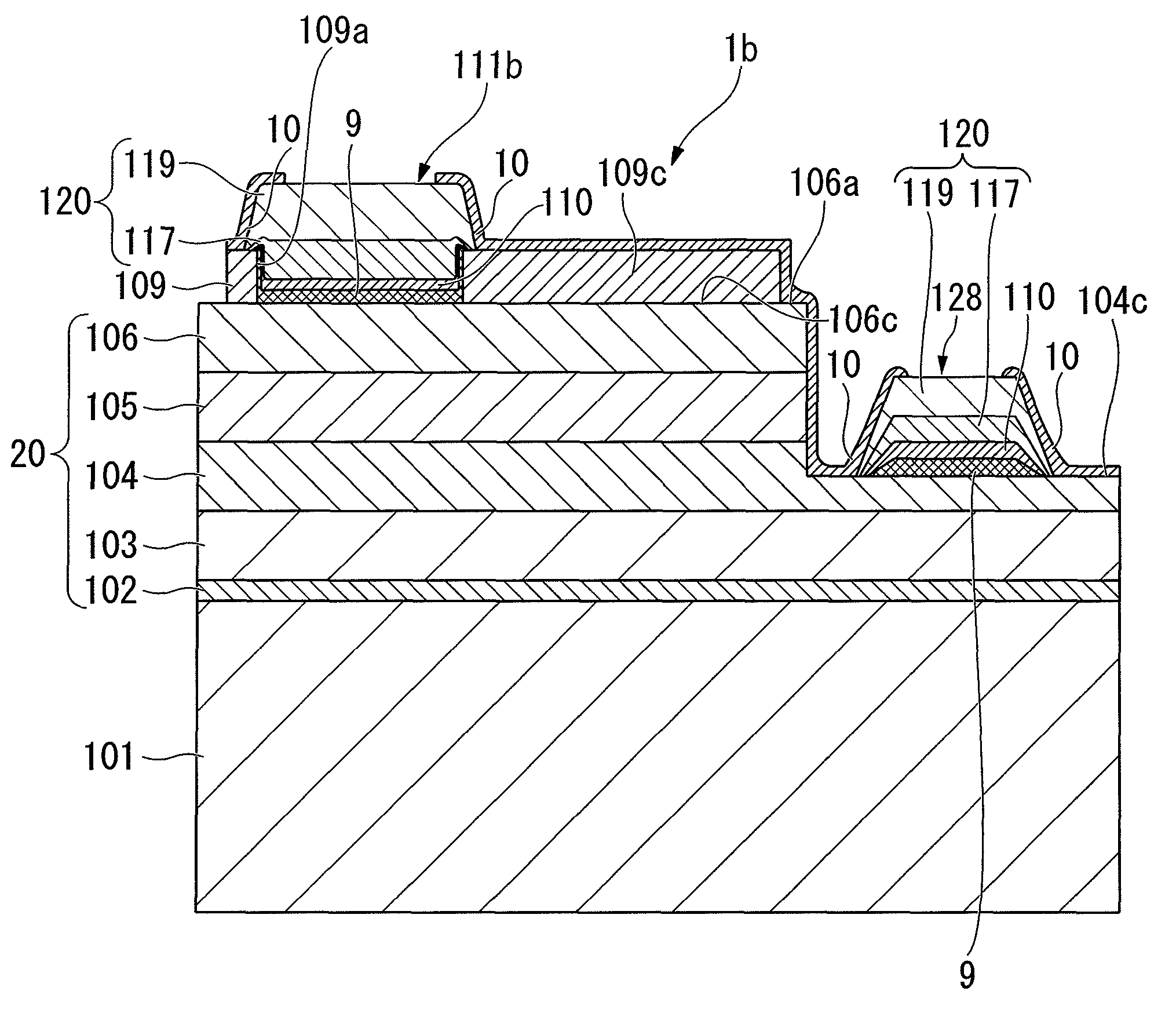
[0236]FIGS. 14 to 17 are views illustrating an example of a semiconductor light-emitting element according to an embodiment of the present invention. FIG. 14 is a schematic cross-sectional view of a semiconductor light-emitting element according to an embodiment of the present invention, and FIG. 15 is a schematic plan view of a semiconductor light-emitting element according to an embodiment of the present invention. FIG. 16 is a schematic cross-sectional view illustrating a laminated semiconductor of a semiconductor light-emitting element according to an embodiment of the present invention, and FIG. 17 is a schematically enlarged cross-sectional view of a p-type electrode of a semiconductor light-emitting element illustrated in FIG. 14 according to an embodiment of the present invention.

[0237]As illustrated in FIG. 14, a semiconductor light-emitting element 1 according to this embodiment includes a substrate 101, a laminated semiconductor layer 20 formed on the substrate 101, a p-t...

embodiment 12

[0282]FIGS. 26 to 29 are views illustrating an example of a semiconductor light-emitting element according to an embodiment of the present invention. FIG. 26 is a schematic cross-sectional view of the semiconductor light-emitting element, and FIG. 27 is a schematic plan view of a semiconductor light-emitting element illustrated in FIG. 26. FIG. 28 is a schematic enlarged cross-sectional view of a laminated semiconductor layer constituting a semiconductor light-emitting element illustrated in FIG. 26. FIG. 29 is a view illustrating an electrode constituting a semiconductor light-emitting element illustrated in FIG. 26, and FIG. 29(a) is a schematic enlarged cross-sectional view of a p-type electrode, and FIG. 29(b) is a schematic enlarged cross-sectional view of an n-type electrode.

[0283]As illustrated in FIG. 26, a semiconductor light-emitting element 1 according to this embodiment includes a substrate 101, a laminated semiconductor layer 20 formed on the substrate 101, a p-type ele...


PUM


Abstract

A semiconductor light-emitting element including a substrate, a laminated semiconductor layer including a light-emitting layer formed over the substrate, one electrode (111) formed over the upper face of the laminated semiconductor layer, and an other electrode formed over the exposed surface of the semiconductor layer, from which the laminated semiconductor layer is partially cut off. The one electrode (111) includes a junction layer (110) and a bonding pad electrode (120) formed to cover the junction layer. The bonding pad electrode has a maximum thickness larger than that of the junction layer, and is composed of one or two or more layers. Slopes (110c), (117c) and (119c), which are made gradually thinner toward the outer circumference, are formed in the outer circumference portions (110d) and (120d) of the junction layer and the bonding pad electrode. Also disclosed is a method for manufacturing the element and a lamp.

Description

BACKGROUND OF THE INVENTION[0001]1. Field of the Invention[0002]The present invention relates to a semiconductor light-emitting element, an electrode and a manufacturing method for the element, and a lamp, and more particularly to a semiconductor light-emitting element having an electrode with improved junction and anticorrosion properties, an electrode and a manufacturing method for the element, and a lamp.[0003]Priority is claimed on Japanese Patent Application No. 2008-157248, filed in the Japan Patent Office on Jun. 16, 2008, Japanese Patent Application No. 2008-199802, filed in Japan Patent Office on Aug. 1, 2008, Japanese Patent Application No. 2008-228133, filed in the Japan Patent Office on Sep. 5, 2008, and Japanese Patent Application No. 2009-133177, filed in the Japan Patent Office on Jun. 2, 2009, the contents of which are incorporated herein by reference.[0004]2. Description of Related Art[0005]Recently, as a semiconductor material for a short-wavelength light-emitting ...

Claims


Application Information

Patent Timeline
Patent Type & Authority Patents(United States)
IPC IPC(8): H01L33/04H01L33/46H01L33/42
CPCH01L33/38H01L33/405H01L33/0095H01L33/32H01L33/42H01L33/44H01L2933/0016H01L2224/73265
Inventor HIRAIWA, DAISUKEOKABE, TAKEHIKOOHBA, REMIWATANABE, MUNETAKA
Owner TOYODA GOSEI CO LTD
Why Eureka
Try Eureka