Semiconductor memory device

a memory device and semiconductor technology, applied in semiconductor devices, digital storage, instruments, etc., can solve the problems of failure of miniaturization of transistors, high manufacturing cost, and high manufacturing cost, and achieve the effect of improving the speed of reading data

Inactive Publication Date: 2013-11-05
SEMICON ENERGY LAB CO LTD
View PDF8 Cites 1 Cited by
  • Summary
  • Abstract
  • Description
  • Claims
  • Application Information

AI Technical Summary

Benefits of technology

[0014]A memory needing refresh operation is also called a volatile memory. Needless to say, there is a variation in charge holding time between memory cells included in the volatile memory. Therefore, the timing of refresh operation in the volatile memory cell is set with a sufficient margin on the basis of the memory cell with the shortest charge holding time so as to prevent all memory cells from causing defects in storage holding so that each memory cell can operate stably. When the number of memory cells in the volatile memory is increased, time needed for refresh operation is increased, which makes it difficult to have a margin for a cycle of the refresh operation.
[0028]The second transistor which controls writing of data to the memory cell is provided to extend from a gate electrode toward a source region of a MOS transistor, whereby an area occupied by one memory cell can be decreased. That is, even in the case where two transistors are needed to form one memory cell, a first transistor and a second transistor are provided to overlap with each other; thus, memory cells can be formed without increasing the area per cell.

Problems solved by technology

In a structure in which a writing transistor with a vertical-channel structure is provided over a source region of a reading transistor, a transistor is formed over another transistor, which causes a problem of doubling the number of manufacturing steps.
However, such a process is extremely difficult, and a large margin is needed according to a design rule, which results in failure of miniaturization of the transistors.
Furthermore, the writing transistor with a vertical-channel structure is formed using a polycrystalline silicon film having many defects, unlike the reading transistor formed using a single crystal silicon substrate, and thus characteristics of the writing transistor are poor.
Specifically, the transistor formed using a polycrystalline silicon film tends to have a large amount of off-state current.
Note that according to Patent Document 3, a semiconductor layer in the transistor is formed by epitaxial growth; however, it is impossible to perform epitaxial growth starting from a contact opening portion in the source region to form a single crystal semiconductor in which a gate electrode is buried.
Even if such a semiconductor film could be deposited, the silicon film has many defects, and thus a favorable transistor cannot be obtained.
When the number of memory cells in the volatile memory is increased, time needed for refresh operation is increased, which makes it difficult to have a margin for a cycle of the refresh operation.

Method used


Image

  • Semiconductor memory device
  • Semiconductor memory device
  • Semiconductor memory device

Examples


Embodiment Construction

[0041]An embodiment of the disclosed invention will be described with reference to drawings. However, the invention to be disclosed is not limited to the embodiment below, and it is easily understood by those skilled in the art that modes and details can be variously changed without departing from the purpose and the scope of the present invention. Therefore, the disclosed invention is not interpreted as being limited to the description of the embodiment below.

[0042]Further, in embodiments hereinafter described, the same parts are denoted with the same reference numerals throughout the drawings. Note that components illustrated in the drawings, that is, a thickness or a width of a layer, a region, or the like, a relative position, and the like are exaggerated in some cases for clarification in description of embodiments.

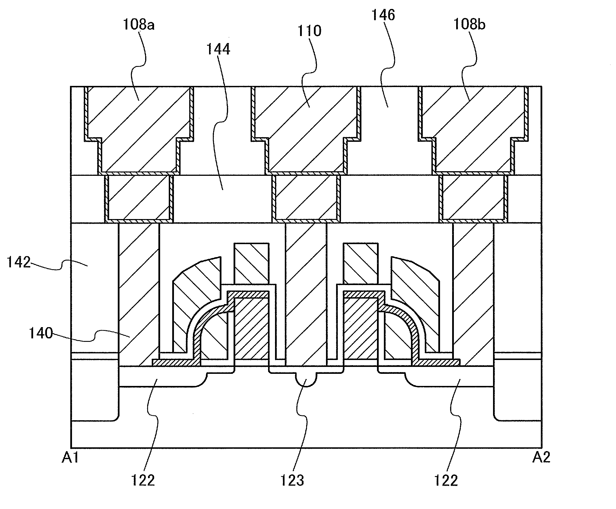
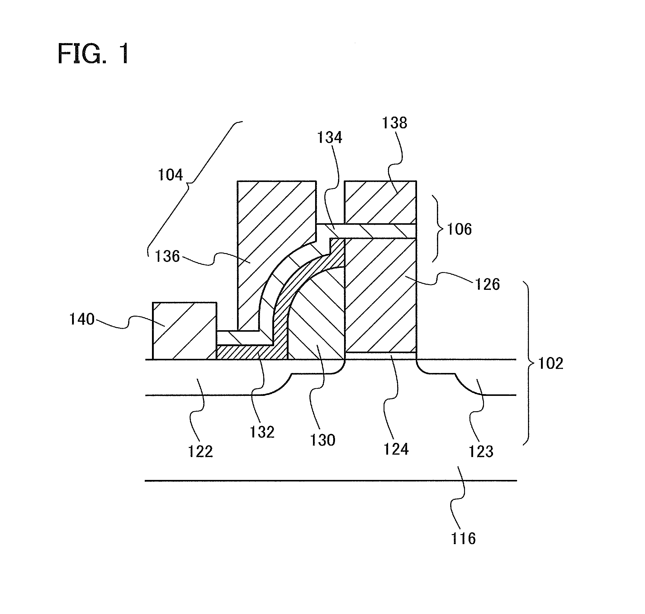
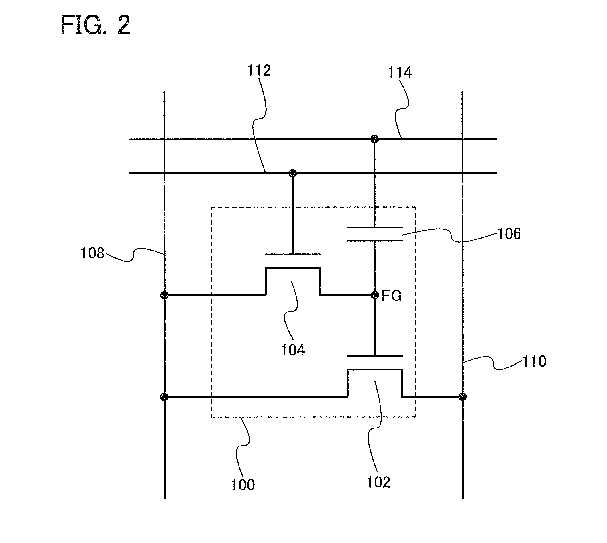
[0043]A semiconductor memory device according to one embodiment of the present invention will be described with reference to FIG. 1 and FIG. 2. FIG. 1 schematically ...


PUM


Abstract

An object is to provide a semiconductor memory device which can be miniaturized and also secures a sufficient margin for the refresh period. A memory cell includes a reading transistor, a writing transistor, and a capacitor. In the above structure, the capacitor controls a potential applied to a gate of the reading transistor. The writing transistor controls writing and erasing of data and, when the transistor is off, has small current so that loss of electric charges stored in the capacitor, which is due to leakage current of the writing transistor, can be prevented. A semiconductor layer included in the writing transistor is provided so as to extend from the gate electrode toward a source region of the reading transistor. The capacitor is provided to overlap with the gate electrode of the reading transistor.

Description

BACKGROUND OF THE INVENTION[0001]1. Field of the Invention[0002]An embodiment of the present invention relates to a semiconductor memory device. An embodiment of the invention to be disclosed includes a structure of a memory cell and a structure of an element included in the memory cell.[0003]2. Description of the Related Art[0004]As a memory cell in a semiconductor memory, one including two transistors (a reading transistor and a writing transistor), one capacitor, and one diode is known (for example, see Patent Document 1 and Patent Document 2). In this memory cell, a gate of the reading transistor is connected to the capacitor, and the writing transistor connected to a bit line for writing controls the charge and discharge of the capacitor. With this structure, storage and erasing of data is performed.[0005]It is only necessary that the capacitor in the above memory cell has capacitance high enough to turn the reading transistor on; thus, the capacitor in the above memory cell ha...

Claims


Application Information

Patent Timeline
Patent Type & Authority Patents(United States)
IPC IPC(8): H01L27/105H01L21/16
CPCH01L27/1156G11C11/403H01L27/1225G11C16/0433H10B41/70H10B99/00H10B12/00
Inventor ARAI, YASUYUKI
Owner SEMICON ENERGY LAB CO LTD
Why Eureka
Try Eureka