Method of manufacturing semiconductor device

a manufacturing method and semiconductor technology, applied in the direction of semiconductor devices, electrical devices, transistors, etc., can solve the problems of reducing the threshold voltage at the end portion, reducing the oxidation rate, and prolonging so as to reduce the heat treatment time, reduce the diffusion of impurities, and reduce the heat treatment temperature

Inactive Publication Date: 2009-11-05
RENESAS TECH CORP
View PDF4 Cites 17 Cited by
  • Summary
  • Abstract
  • Description
  • Claims
  • Application Information

AI Technical Summary

Benefits of technology

[0008]A diffusion length of impurities such as phosphorus (P) and boron (B) introduced into a silicon substrate is determined by a square root of a product of a diffusion coefficient of the impurity (heat treatment temperature) and a heat treatment time. That is, from the view point of suppressing the diffusion of impurities, it is desirable to realize a lowering of heat treatment temperature and a reduction of heat treatment time in a heat treatment process performed on the silicon substrate after introducing the impurities. If a lowering of heat treatment temperature and a reduction of heat treatment time can be realized, it is possible to make the diffusion of impurities small, and as a result, a variation of impurity concentration (the number of impurities) can be made small.

Problems solved by technology

Thus, a problem of threshold voltage lowering at the end portions of the channel region CH occurs.
The lowering of the oxidation rate means the lengthening of the heat treatment time.

Method used


Image

  • Method of manufacturing semiconductor device
  • Method of manufacturing semiconductor device
  • Method of manufacturing semiconductor device

Examples


first embodiment

[0060]Prior to describing embodiments of the present invention, a basic concept of the present invention will be described. The basic concept of the present invention lies in that a silicon oxide film is formed by thermal reaction made by generating a large amount of oxygen radicals having a large reactivity without using plasma. More specifically, in the case of using plasma, there are not only radical species but also ion species present in the plasma. Therefore, the formed silicon oxide film becomes prone to be damaged due to a sputtering phenomenon by the ion species during forming the silicon oxide film. From this reason, the formed silicon oxide film is frequently damaged in the method of using plasma, and it is thus difficult to form a highly reliable silicon oxide film. On the contrary, according to the present invention, a highly reliable silicon oxide film is formed by performing a thermal oxidation using oxygen radicals having a large reactivity and containing no ion spec...

second embodiment

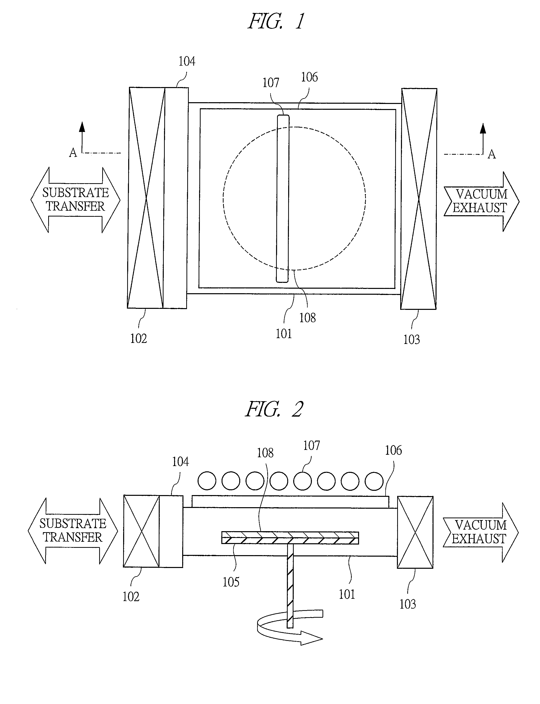
[0088]Next, a second embodiment will be described in detail. Herein, a film thickness uniformity of a thermal oxide film (silicon oxide film) to be obtained in the second embodiment will be described. In the case of using the heat treatment apparatus (oxidation apparatus) illustrated in FIG. 1 and FIG. 2 to carry out a thermal oxidation method by ozone (O3) and hydrogen chloride (HCl), uniformity of the thermal oxide film greatly differs depending on a supplying method of the source gases (ozone (O3) and hydrogen chloride (HCl)). More specifically, in the case of supplying ozone (O3) and hydrogen chloride (HCl) from the gas introduction block 104 illustrated in FIG. 1 and FIG. 2, the thickness of the obtained thermal oxide film (silicon oxide film) is greatly changed depending on respective gas introduction positions and the number of introduction lines.

[0089]FIG. 8A and FIG. 8B are diagrams illustrating positional relationships of a semiconductor wafer (semiconductor substrate) and...

third embodiment

[0097]In the following, a thermal oxidation method according to a third embodiment will be described in detail with reference to the accompanied drawings. In the third embodiment, a single silicon substrate (resistivity: 10 Ω·cm) and a SiC substrate (4H) each having different orientations and a polycrystalline silicon film, a non-doped polycrystalline SiC film and a silicon nitride film (Si3N4 film) each having different impurities were prepared and each substrate or each thin film was oxidized in the same conditions, and a film thickness ratio of a silicon oxide film obtained thereby was evaluated.

[0098]The polycrystalline silicon film was formed by depositing a noncrystalline silicon film by a low pressure CVD (Chemical Vapor Deposition) method using disilane (Si2H6) as a source gas and then crystallizing the noncrystalline silicon film by a heat treatment. Disilane (Si2H6) and phosphine (PH3) were used for a phosphorus-doped noncrystalline silicon film, and disilane (Si2H6) and d...


PUM


Abstract

A thermal oxidation method capable of obtaining a high oxidation rate by generating a sufficient enhanced-rate oxidation phenomenon even in a low temperature region is provided. In addition, a thermal oxidation method capable of forming a silicon oxide film having a high reliability even when formed at a low temperature region. A basic concept herein is to form a silicon oxide film by thermal reaction by generating a large amount of oxygen radicals (O*) having a large reactivity without using plasma. More specifically, ozone (O3) and other active gas are reacted, so that ozone (O3) is decomposed highly efficiently even in a low temperature region, thereby generating a large amount of oxygen radicals (O*). For example, a compound gas containing a halogen element can be used as the active gas.

Description

CROSS-REFERENCE TO RELATED APPLICATION[0001]The present application claims priority from Japanese Patent Application No. JP 2008-119540 filed on May 1, 2008, the content of which is hereby incorporated by reference into this application.TECHNICAL FIELD OF THE INVENTION[0002]The present invention relates to a technique for manufacturing a semiconductor device. More particularly, the present invention relates to a technique effectively applied to a technique for forming a silicon oxide film having a sufficiently large thickness at a relatively low temperature in the case of forming a silicon oxide film having a high reliability by a thermal oxidation method.BACKGROUND OF THE INVENTION[0003]Along with miniaturization of silicon (Si) semiconductor devices, variations in threshold voltages among respective devices (respective MISFETs (Metal Insulator Semiconductor Field Effect Transistors)) have been increased and it has been a big problem in the stable operation of the devices. This is ...

Claims


Application Information

Patent Timeline
Patent Type & Authority Applications(United States)
IPC IPC(8): H01L21/336H01L21/22H01L21/762
CPCH01L21/76224H01L29/7833H01L29/6659
Inventor MINE, TOSHIYUKIHAMAMURA, HIROTAKA
Owner RENESAS TECH CORP
Why Eureka
Try Eureka