Lateral super junction device with high substrate-drain breakdown and built-in avalanche clamp diode

a super junction device and substrate technology, applied in the direction of semiconductor devices, basic electric elements, electrical apparatus, etc., can solve the problems of limited manufacturing ease and cost of conventional vertical high voltage power devices implemented with super-junction structures, and inability to achieve a high density of alternately doped columns

Active Publication Date: 2013-11-05
ALPHA & OMEGA SEMICON INC
View PDF6 Cites 35 Cited by
  • Summary
  • Abstract
  • Description
  • Claims
  • Application Information

AI Technical Summary

Benefits of technology

[0008]It is another aspect of this invention to provide a new and improved device structure and manufacturing method to form the junction field effect transistor (JFET) power device such that a vertical PN diode is incorporated between drain and substrate below allowing unclamped inductive switching performance to be improved. The substrate may be at gate potential, having a gate metal on its bottom side.
[0010]It is another aspect of this invention to provide a new and improved device structure and manufacturing method to form the junction field effect transistor (JFET) power device such that the structure and configuration of the JFET device includes a buried N− buffer layer below the deep drain column. The peak electric field under the drain can be significantly reduced minimizing the E-field increase due to the cylindrical junction between the drain trench and the substrate. With the reduction of electrical field crowding, the breakdown voltage can be further increased.

Problems solved by technology

However, the manufacturing technologies and device configuration for implementing the super-junction structures in the MOSFET devices are still confronted with manufacturability difficulties.
The manufacturing ease and cost of the conventional vertical high voltage power devices implemented with super-junction structures are limited due to the structural features that require numerous time-consuming, complex, and expensive manufacturing processes.
Achieving a high density of alternately doped columns becomes prohibitive since it requires a direct increase in the number of these steps.
It is difficult and costly to manufacture the vertical charge-balanced alternately doped columns of FIG. 1A, especially at high densities.
However, a typical device configuration as shown in FIG. 1B is limited by its drain-substrate breakdown voltage and is further restricted due to the difficulty in improving its unclamped inductive switching (UIS). FIG. 1C shows an example of another lateral super junction device as disclosed by Tatsuhiko Fujihira in the same paper as mentioned above, “Theory of Semiconductor Superjunction Devices”.
This device suffers from excessive channel resistance in distributing the current into the stacked n-type conduction paths.

Method used


Image

  • Lateral super junction device with high substrate-drain breakdown and built-in avalanche clamp diode
  • Lateral super junction device with high substrate-drain breakdown and built-in avalanche clamp diode
  • Lateral super junction device with high substrate-drain breakdown and built-in avalanche clamp diode

Examples


Embodiment Construction

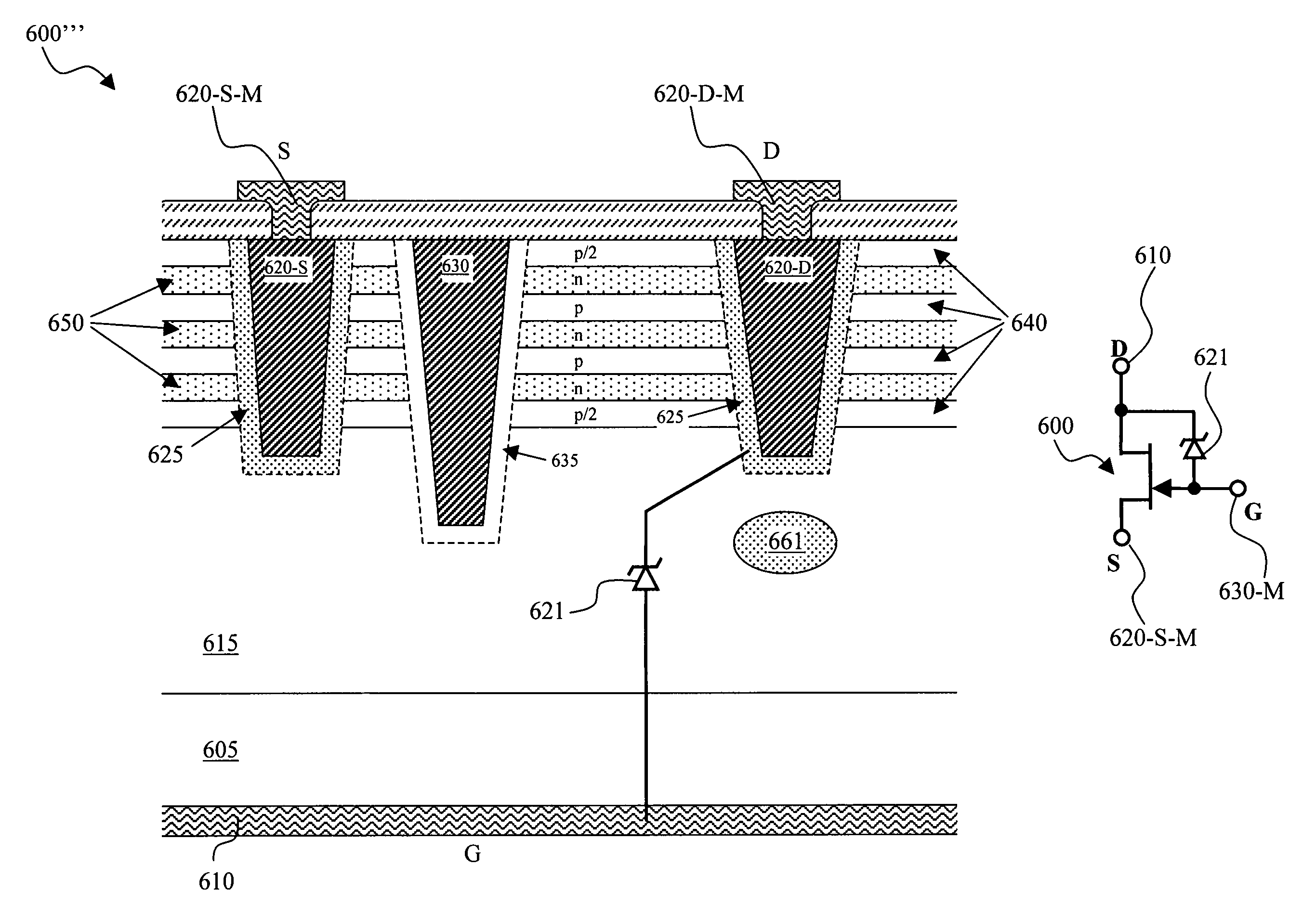
[0034]Referring to FIG. 2 for a cross sectional view of a lateral power device 100 that illustrates the new concepts including the new structural and manufacturing features of this invention. The lateral power device 100 is supported on a P+ substrate 105 that includes a gate metal electrode 110 disposed on the bottom of the substrate. The P+ substrate 105 may further comprise a P Epi layer 106 on top of it. The lateral power device 100 includes a source and a drain formed as N+ column 120-S and N+ column 120-D, respectively, disposed in a first and second trench at two opposite sides of the semiconductor substrate. A P+ doped column 130 disposed in another trench functions as a gate of the lateral power device. The P+ doped column 130 connects to the P-Epi 106, thus the P+ substrate 105 is biased to the gate, and a gate metal 110 may be located at the bottom of P+ substrate 105 to control the gate column 130. The source and drain 120-S and 120-D may be formed with N+ doped polysili...


PUM


Abstract

This invention discloses configurations and methods to manufacture lateral power device including a super-junction structure with an avalanche clamp diode formed between the drain and the gate. The lateral super-junction structure reduces on-resistance, while the structural enhancements, including an avalanche clamping diode and an N buffer region, increase the breakdown voltage between substrate and drain and improve unclamped inductive switching (UIS) performance.

Description

BACKGROUND OF THE INVENTION[0001]1. Field of the Invention[0002]The invention relates generally to semiconductor power devices. More particularly, this invention relates to configurations and methods to manufacture lateral power device including a super-junction structure with an avalanche clamp diode formed between the drain and the gate. The lateral super-junction structure reduces on-resistance, while the structural enhancements increase the breakdown voltage between substrate and drain and improve unclamped inductive switching (UIS) performance.[0003]2. Description of the Prior Art[0004]Conventional semiconductor power device such as the MOSFET power devices implemented with a super-junction structure can achieve performance improvements with significant reduction of the on-resistance while still maintaining a high breakdown voltage. However, the manufacturing technologies and device configuration for implementing the super-junction structures in the MOSFET devices are still con...

Claims


Application Information

Patent Timeline
Patent Type & Authority Patents(United States)
IPC IPC(8): H01L29/66H01L21/00
CPCH01L27/0705H01L29/0634H01L29/66901H01L29/808H01L2224/48091H01L2224/48247H01L2924/181H01L2224/0603H01L2224/48257H01L2924/13091H01L2924/00014H01L2924/00012H01L2924/00
Inventor BOBDE, MADHURBHALLA, ANUPYILMAZ, HAMZAMA, WILSONGUAN, LINGPENGLEE, YEEHENGCHEN, JOHN
Owner ALPHA & OMEGA SEMICON INC
Why Eureka
Try Eureka