
Fabricating method of embedded package structure

a technology of packaging structure and manufacturing method, which is applied in the direction of cable/conductor manufacturing, printed circuit aspects, chemistry apparatus and processes, etc., can solve the problems of insufficient or excessive etching, short circuits or open circuits in patterned circuits, embedded elements b>100/b> cannot be used anymore, etc., to achieve the effect of improving manufacturing yield and reliability

Active Publication Date: 2013-11-12
UNIMICRON TECH CORP
View PDF40 Cites 3 Cited by
  • Summary
  • Abstract
  • Description
  • Claims
  • Application Information

AI Technical Summary

Benefits of technology

The present invention is a method for making an embedded package structure that improves manufacturing yield and reliability. The method involves forming circuit structures on separate boards and bonding them together with an isolation layer. The circuit substrates and a semi-cured film are then laminated, and the embedded element is encapsulated in the film. This reduces the risk of damage to the embedded element and achieves high yield of circuits and high reliability of the overall package structure.

Problems solved by technology

Therefore, in a subsequently-performed etching process, inaccurate photoresist development, insufficient exposure, or excessive exposure is likely to bring about incomplete or excessive etching, thus resulting in short circuits or open circuits in the patterned circuits.
As a result, the embedded element 100 can no longer be used and has to be thrown away.
Alternatively, electrical properties of the embedded element 100 may be fatally damaged.

Method used


Image

  • Fabricating method of embedded package structure
  • Fabricating method of embedded package structure
  • Fabricating method of embedded package structure

Examples


Embodiment Construction

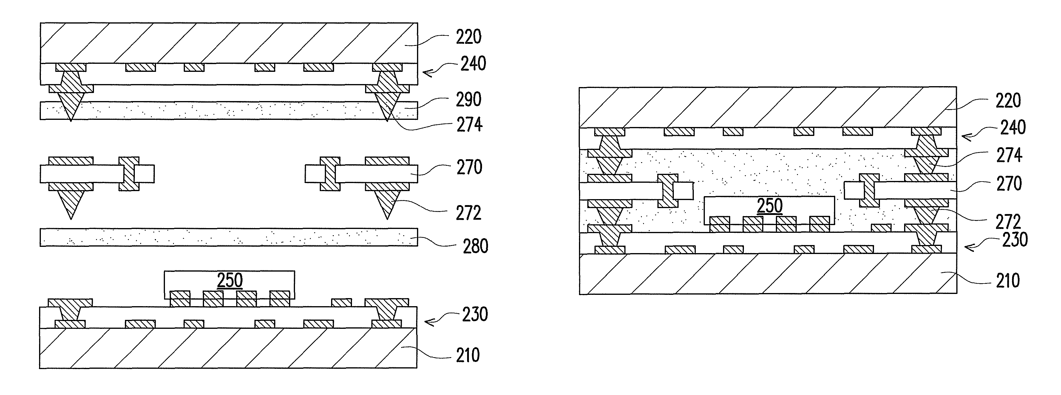
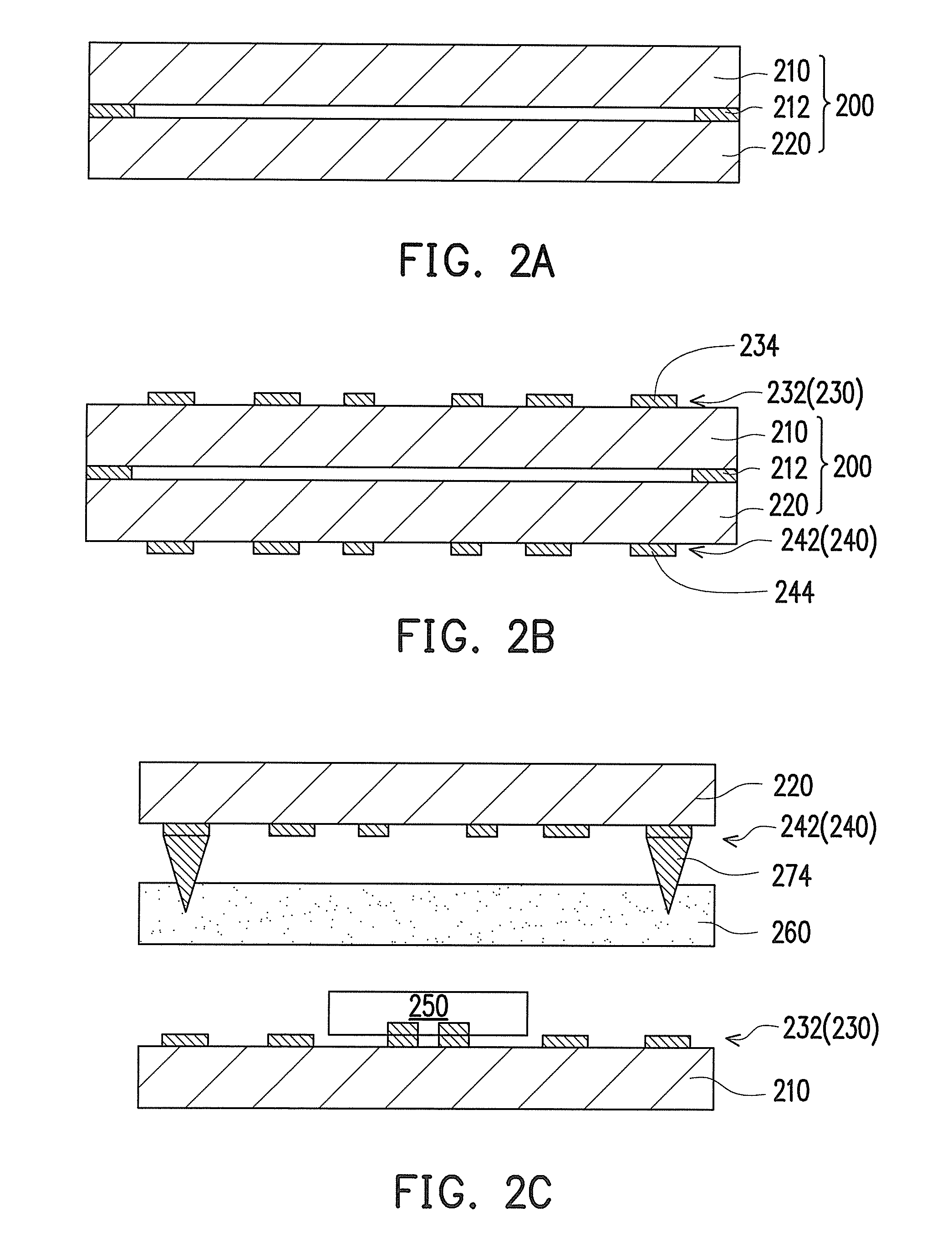
[0027]FIGS. 2A˜2G are schematic views illustrating a fabricating method of an embedded package structure according to an embodiment of the present invention. As indicated in FIGS. 2A and 2B, a first circuit structure 230 and a second circuit structure 240 are respectively formed on a first board 210 and a second board 220 that are combined to form an integrated panel 200. In the present embodiment, the first circuit structure 230 is formed by first fabricating a first circuit layer 232 on the first board 210. Here, the first circuit layer 232 can be formed by, for example, performing an additive process, performing a semi-additive process, patterning and etching a metal layer (e.g. copper foil), or performing a jet-printing process, performing a transfer printing process, and so on. Besides, the first circuit layer 232 includes at least one interconnect pad 234. Similar to the process of forming the first circuit layer 232 (230), a process of forming the second circuit substrate 240...


PUM

PropertyMeasurementUnit
diameteraaaaaaaaaa
heightaaaaaaaaaa
conductiveaaaaaaaaaa

Abstract

A fabricating method of an embedded package structure is provided. The method includes combining a first board and a second board to form an integrated panel; forming a first circuit structure on the first board and forming a second circuit structure on the second board; separating the first board from the second board; electrically disposing an embedded element on the first circuit structure; forming at least one conductive bump on the second circuit structure; and providing a semi-cured film and performing a laminating process to laminate the first circuit structure on the first board, the semi-cured film, and the second circuit structure on the second board, wherein the semi-cured film encapsulates the embedded element, and after the laminating process is performed, the at least one conductive bump pierces through the semi-cured film and is electrically connected to the first circuit structure.

Description

CROSS-REFERENCE TO RELATED APPLICATION[0001]This application claims the priority benefit of Taiwan application serial no. 98119725, filed Jun. 12, 2009. The entirety of the above-mentioned patent application is hereby incorporated by reference herein and made a part of specification.BACKGROUND OF THE INVENTION[0002]1. Field of the Invention[0003]The present invention relates to a fabricating method of an embedded package structure. More particularly, the present invention relates to a fabricating method of an embedded package structure with multiple layers of circuits.[0004]2. Description of Related Art[0005]FIGS. 1A˜1C are schematic views illustrating a conventional structure having an embedded element and a fabricating method of the conventional structure. First, as shown in FIG. 1A, an embedded element 100 is surface-mounted to two non-patterned metal layers 110 and 120. The two non-patterned metal layers 110 and 120 are laminated respectively to upper and lower sides of a dielec...

Claims


Application Information

Patent Timeline
Patent Type & Authority Patents(United States)
IPC IPC(8): H05K3/20H05K3/00
CPCH01L21/6835H01L24/19H01L24/20H01L24/81H01L24/83H01L24/92H05K1/186H01L23/5389H05K3/4007Y10T29/49124H01L24/16H01L24/32H01L24/73H01L2221/68304H01L2221/68359H01L2221/68363H01L2221/68381H01L2221/68386H01L2224/2919H01L2224/321H01L2224/32225H01L2224/73204H01L2224/81005H01L2224/81903H01L2224/83005H01L2224/83203H01L2224/8385H01L2224/83862H01L2224/9211H01L2924/01013H01L2924/01029H01L2924/01047H01L2924/01079H05K1/187H05K3/4614H05K3/4647H05K2201/10674H05K2203/063Y10T29/49128H01L2924/0665H01L2924/014H01L2924/0105H01L2924/01033H01L2224/81H01L2224/83H01L2224/19H01L2924/00H01L2924/12042H01L2924/14H01L2224/0557H01L2224/05573H01L2924/00014H01L2224/05571H01L2224/0554H01L2224/05599H01L2224/0555H01L2224/0556
Inventor CHEN, TSUNG-YUANTING, MING-HUANG
Owner UNIMICRON TECH CORP
Learn More