Radiation source
- Summary
- Abstract
- Description
- Claims
- Application Information
AI Technical Summary
Benefits of technology
Problems solved by technology
Method used
Image
Examples
Example
DETAILED DISCUSSION IN CONJUNCTION WITH THE DRAWINGS
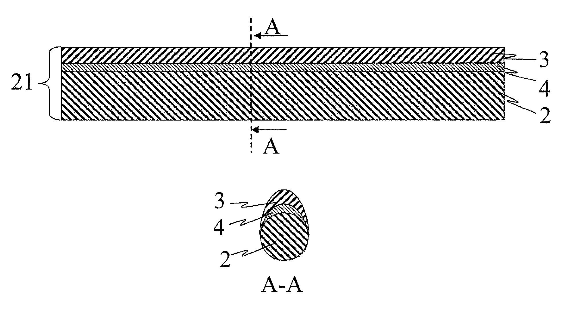
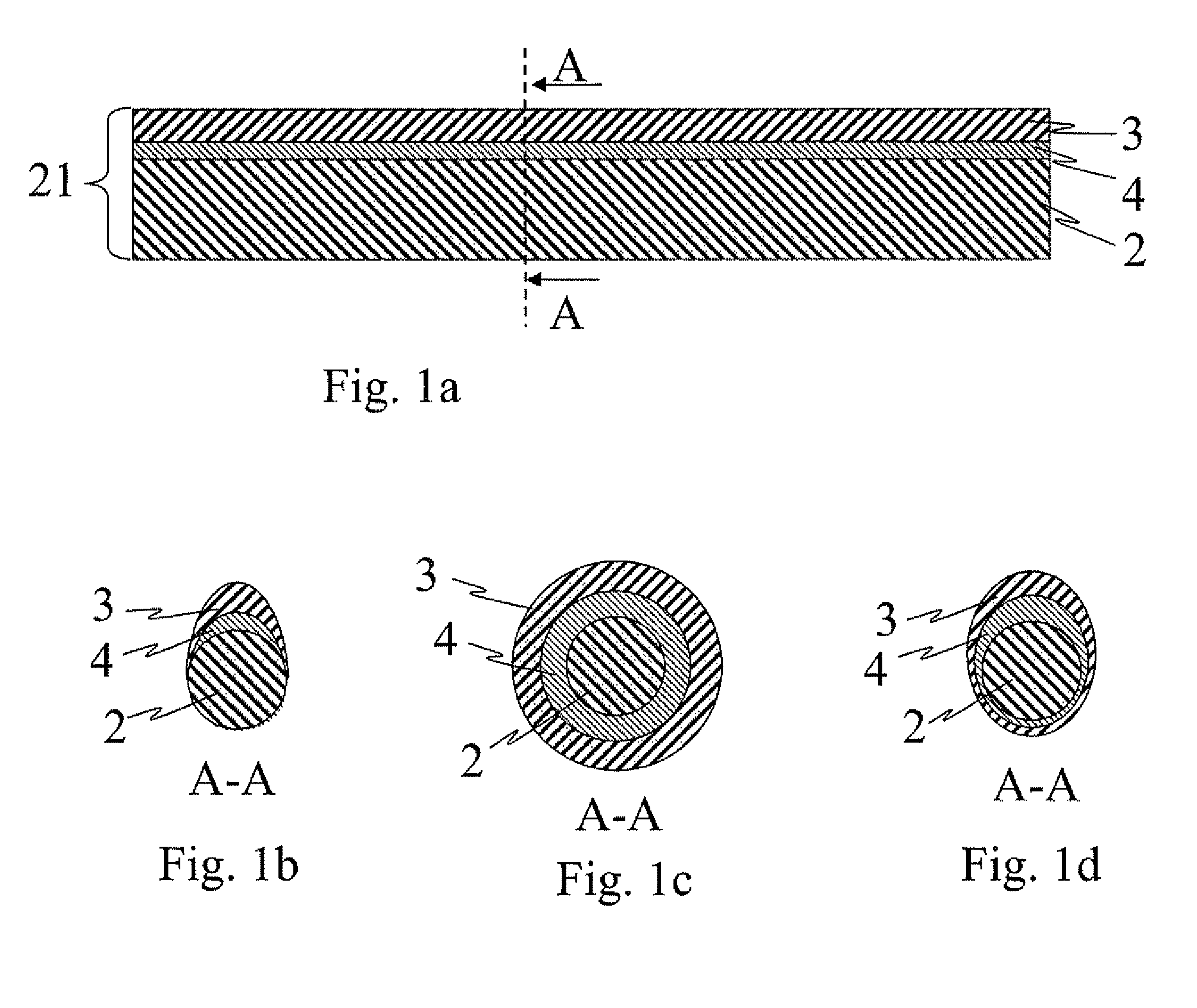
[0031]FIG. 1a shows the construction of a coated source element 21 schematically in a section along one of the longitudinal axes of the plane containing the source element 2. The infrared radiation emitting source element 2 is a silicon carbide fiber. A fiber is understood, in such case, to be a very thin element, whose length exceeds its diameter by a number of orders of magnitude. The diameter of source element 2 is as small as possible and lies, for example, between 50 and 300 micrometers, preferably between 50 and 150 micrometers.
[0032]Source element 2 has two coatings 3, 4, wherein the outer coating is a metal coating 3, which functions as a heating element and, consequently, is characterized by a high electrical resistance. The intermediate layer 4 arranged under metal coating 3 is a adhesion promoting layer, which leads to an improved adhesion of metal coating 3 to the silicon carbide fiber. Intermediate layer 4 can also be ...
PUM
| Property | Measurement | Unit |
|---|---|---|
| Thickness | aaaaa | aaaaa |
| Thickness | aaaaa | aaaaa |
| Diameter | aaaaa | aaaaa |
Abstract
Description
Claims
Application Information


