Memory apparatus and associated method

a memory apparatus and associated method technology, applied in the field of memory apparatus, can solve the problems of frequent damage to the bit column of the memory apparatus, and achieve the effect of increasing the yield rate of the memory apparatus and promoting data access failur

Active Publication Date: 2013-12-24
XUESHAN TECH INC
View PDF7 Cites 0 Cited by
  • Summary
  • Abstract
  • Description
  • Claims
  • Application Information

AI Technical Summary

Benefits of technology

[0004]According to the present disclosure, a memory apparatus for recovering damage to increase a yield rate of the memory apparatus and even an overall chip is provided. Memory units for constructing a memory space in the memory apparatus are arranged as a plurality of byte rows and bit columns. In practice, damage frequently occurs in bit columns of the memory apparatus. For example, particle pollution in a semiconductor fabrication may cause damage of a whole bit column thereby promoting failing in accessing data. A simple-structured circuit is provided to replace / recover such type of damage.
[0006]The switch circuit selects either the first latching device or the second latching device for outputting bits according to a matching result of an access column address and at least one predetermined column address. The address matcher coupled to the switch circuit controls selection of the latching device for outputting bits. The address matcher in sequence regards the column addresses of the plurality of first bit columns as the access column address, and matches each of the access column addresses with each of the at least one predetermined column address, so that the switch circuit can select either the first latching device or the second latching device for outputting bits according to the matching result of each of the access column addresses and each of the at least one predetermined column address. When one access address matches with the at least one predetermined column address, the switch circuit outputs bits via the second latching device; otherwise, the switch circuit outputs bits via the first latching device. In an embodiment, the at least one predetermined column address is stored into a non-volatile memory.

Problems solved by technology

In practice, damage frequently occurs in bit columns of the memory apparatus.
For example, particle pollution in a semiconductor fabrication may cause damage of a whole bit column thereby promoting failing in accessing data.

Method used


Image

  • Memory apparatus and associated method
  • Memory apparatus and associated method
  • Memory apparatus and associated method

Examples


Embodiment Construction

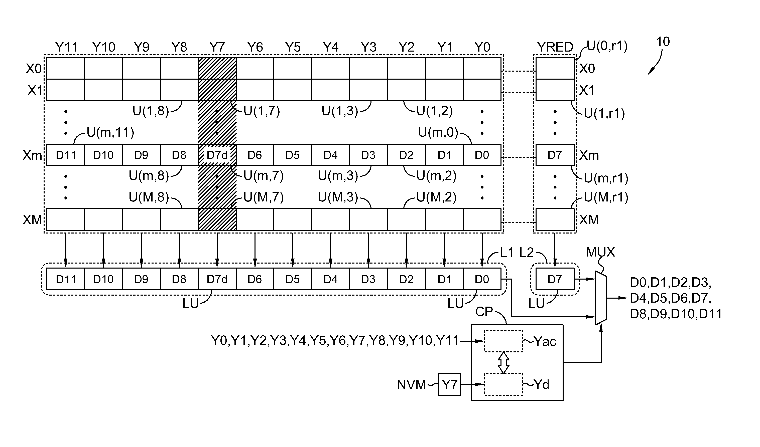
[0020]FIG. 1 is a schematic diagram of a memory apparatus 10 in accordance with an embodiment of the present invention. The memory apparatus 10 is defined in a chip (not shown) comprising a plurality of memory units, which are respectively arranged as a plurality of bit columns and a plurality of bit rows. In FIG. 1, bit columns Y0 to Y11 represent a plurality of bit columns, a plurality of byte rows are represented by byte rows X0, X1 to Xm, and Xm to XM. Each of the bit columns Y0 to Y11 comprises a plurality of memory units, which correspond to a same column address and respectively correspond to one of the byte rows X0 to XM. For example, memory units U(1, 2), U(m, 2) and U(M, 2) correspond to a column address of the bit column Y2, while memory units U(1, 3), U(m, 3) and U(M, 3) correspond to a column address of the bit column Y3. Memory units U(1, 2), U(1, 3), U(1, 7) and U(1, 8) in the bit columns Y2, Y3, Y7 and Y8 correspond to a byte row X1, and memory units U(m, 2), U(m, 3)...


PUM


Abstract

A memory apparatus includes a plurality of first bit columns for constructing a common memory space and at least one reserve second bit column. A column address of a damaged first bit column is recorded as a predetermined column address. When a byte column is accessed, data recorded in the first bit columns and the second bit columns are respectively latched in a first latching device and a second latching device. In the event that the latched access data is accessed, data is outputted by comparing the predetermined column address of each first bit column and an access column address, and when the access column address matches with the predetermined column address, data is outputted via the second latching device; otherwise, the data is outputted via the first latching device.

Description

CROSS REFERENCE TO RELATED PATENT APPLICATION[0001]This patent application is based on Taiwan, R.O.C. patent application No. 099117301 filed on May 28, 2010.FIELD OF THE INVENTION[0002]The present invention relates to a memory apparatus and associated method, and more particularly, to a memory apparatus and associated method capable of recovering / replacing a damaged bit column to increase a yield rate.BACKGROUND OF THE INVENTION[0003]A chip is a most important hardware component in a modern electronic system. Since functions of the chip have become more and more diversified and complicated, a memory apparatus built in the chip has been adopted to support a memory space for operating the chip. However, a yield rate of the chip is reduced due to damage of the memory apparatus.SUMMARY OF THE INVENTION[0004]According to the present disclosure, a memory apparatus for recovering damage to increase a yield rate of the memory apparatus and even an overall chip is provided. Memory units for ...

Claims


Application Information

Patent Timeline
Patent Type & Authority Patents(United States)
IPC IPC(8): G11C7/00
CPCG11C29/846
Inventor HSIEH, WEN PINHSIEH, MENG HSUN
Owner XUESHAN TECH INC
Why Eureka
Try Eureka