Method for sidewall spacer line doubling using atomic layer deposition of a titanium oxide

a technology of titanium oxide and sidewall spacer, applied in the field of nanotechnology, can solve problems such as the fundamental printing limits of current photolithography

Inactive Publication Date: 2014-01-07
WESTERN DIGITAL TECH INC
View PDF12 Cites 248 Cited by
  • Summary
  • Abstract
  • Description
  • Claims
  • Application Information

AI Technical Summary

Problems solved by technology

Current photolithography has reached fundamental printing limits.

Method used


Image

  • Method for sidewall spacer line doubling using atomic layer deposition of a titanium oxide
  • Method for sidewall spacer line doubling using atomic layer deposition of a titanium oxide
  • Method for sidewall spacer line doubling using atomic layer deposition of a titanium oxide

Examples


Embodiment Construction

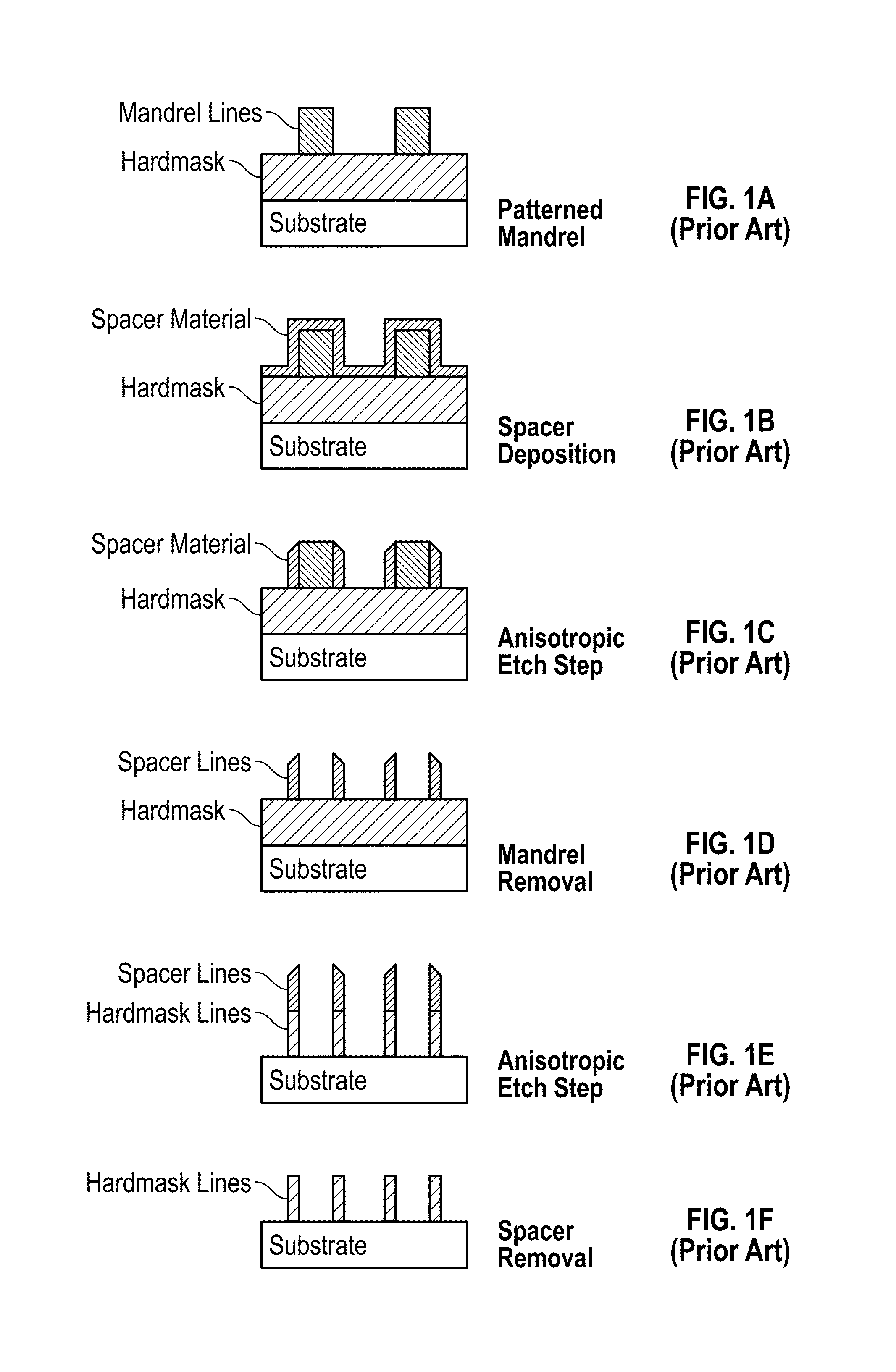
[0012]Atomic layer deposition (ALD) is a thin film deposition process that is based on the sequential use of a gas phase chemical process, in which by repeatedly exposing gas phase chemicals known as the precursors to the growth surface and activating them at elevated temperature, with or without the assistance from a plasma or ozone, a precisely controlled thin film is deposited in a conformal manner. If plasma is involved in the deposition, the technique is referred to as “plasma-enhanced” ALD, or PEALD. If ozone is used in the deposition, the process is called “ozone-assisted” ALD. PEALD and ozone-assisted ALD are both referred to as “energy-assisted” ALD. When the precursors are activated without additional energy assistance from plasma or ozone, the technique would be referred to as “thermal” ALD.

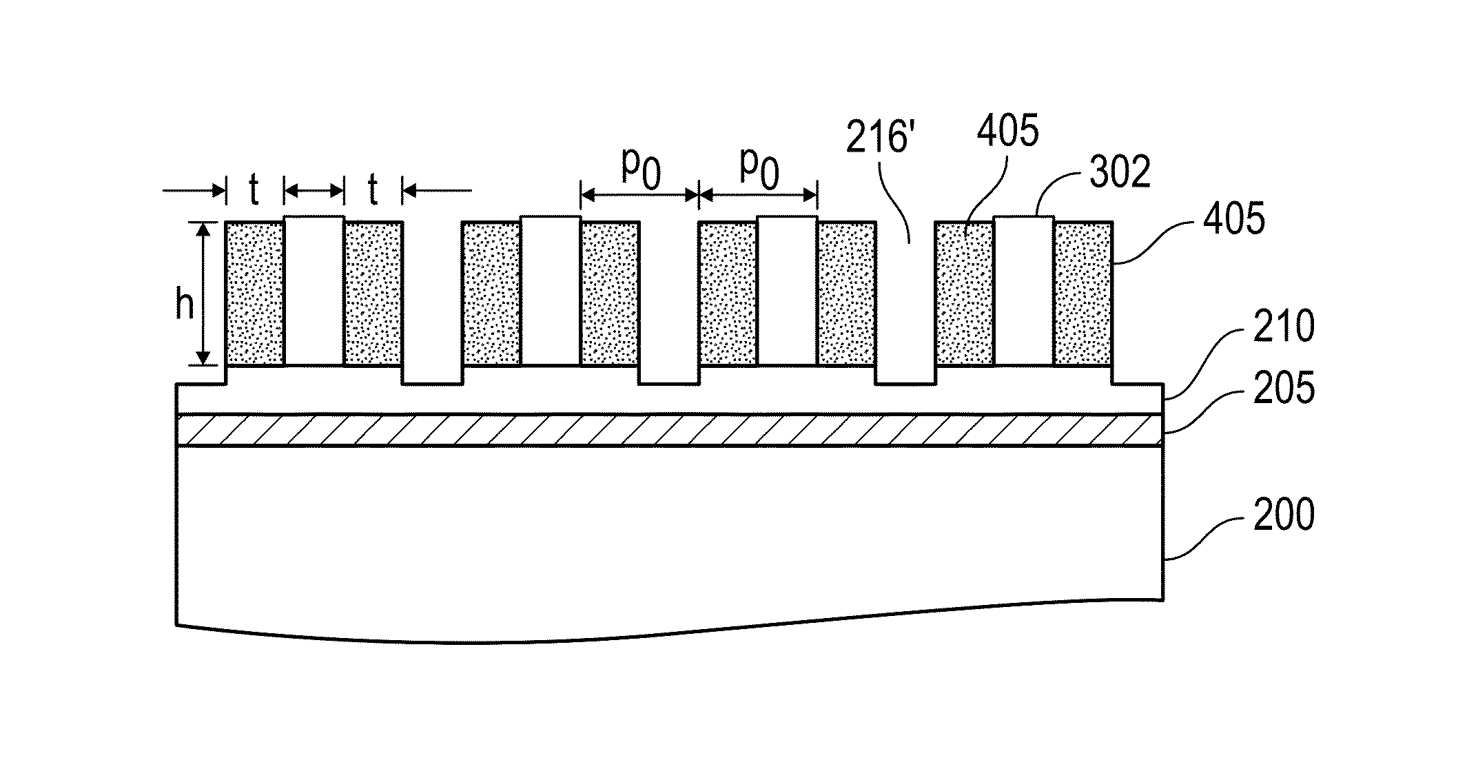
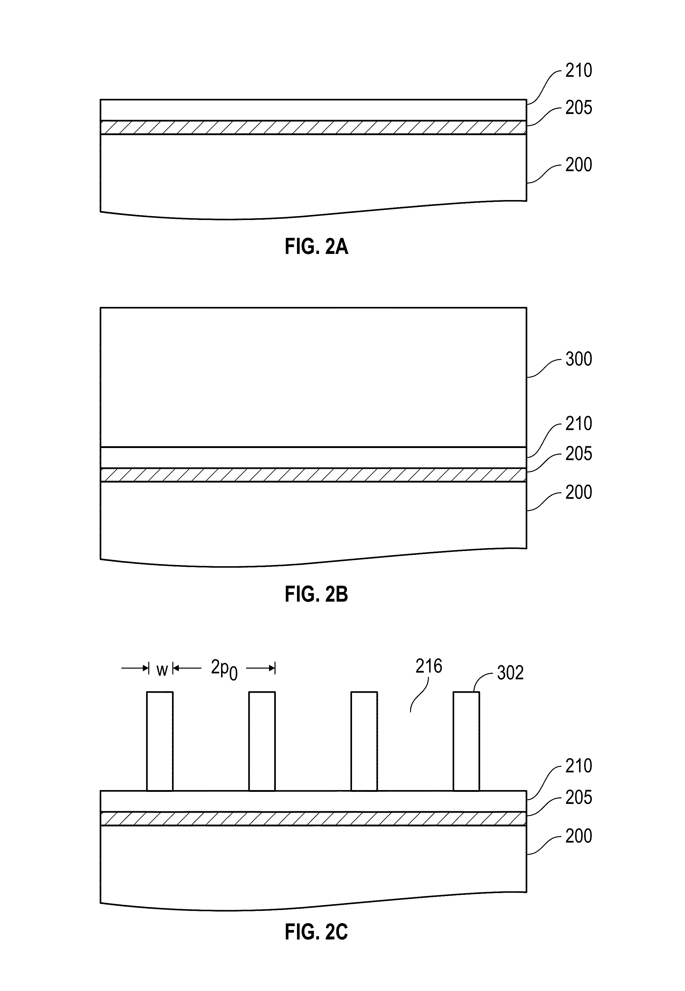
[0013]In the method of this invention, it has been discovered that conformal coating of a titanium oxide (TiOx) spacer material over mandrel lines of diamond-like carbon (DLC) occurs w...


PUM

PropertyMeasurementUnit
temperatureaaaaaaaaaa
thicknessaaaaaaaaaa

Abstract

A method for sidewall spacer line doubling uses thermal atomic layer deposition (ALD) of a titanium oxide (TiOx) spacer layer. A hardmask layer is deposited on a suitable substrate. A mandrel layer of diamond-like carbon (DLC) is deposited on the hardmask layer and patterned into stripes with tops and sidewalls. A layer of TiOx is deposited, by thermal ALD without the assistance of plasma or ozone, on the tops and sidewalls of the mandrel stripes. Thermal ALD of the TiO2, without energy assistance by plasma or ozone, has been found to cause no damage to the DLC mandrel stripes. After removal of the TiOx from the tops of the mandrel stripes and removal of the mandrel stripes, stripes of TiO2 are left on the hardmask layer and may be used as an etch mask to transfer the pattern into the hardmask layer.

Description

BACKGROUND OF THE INVENTION[0001]1. Field of the Invention[0002]This invention relates to line density multiplication in the area of nanotechnology, such as the fabrication of semiconductor devices and nanoimprint templates.[0003]2. Description of the Related Art[0004]Current photolithography has reached fundamental printing limits. One process that is gaining recognition for use in DRAM and NAND flash manufacturing is sidewall spacer “line doubling”, sometimes also referred to as “line multiplication”, “frequency doubling”, or “pitch-halving”. The process also has application in making nanoimprint templates, which may be used for making bit-patterned-media magnetic recording disks, for example as described in U.S. Pat. No. 7,758,981 B2 which is assigned to the same assignee as this application.[0005]The process uses sidewall spacers to create patterned hardmasks as a means of doubling the printed line density. The process is illustrated in FIGS. 1A-1F. A layer of hardmask material ...

Claims


Application Information

Patent Timeline
Patent Type & Authority Patents(United States)
IPC IPC(8): H01L21/311
CPCH01L21/311H01L21/0228H01L21/02186H01L21/0337
Inventor GAO, HELILLE, JEFFREY S.PATEL, KANAIYALAL CHATURDAS
Owner WESTERN DIGITAL TECH INC
Why Eureka
Try Eureka