Supercharge Your Innovation With Domain-Expert AI Agents!

Method and system for fabricating ion-selective field-effect transistor (ISFET)

a field-effect transistor and selective field-effect technology, applied in the direction of material analysis, measurement devices, instruments by electric/magnetic means, etc., can solve the problem of low sensitivity and achieve the effect of enhancing the stabilization of one or more acceptors

Inactive Publication Date: 2014-02-04
MOHAJERZADEH SHAMSODDIN +2
View PDF22 Cites 4 Cited by
  • Summary
  • Abstract
  • Description
  • Claims
  • Application Information

AI Technical Summary

Benefits of technology

The patent text describes a technology that can create a layer of nanopores on a certain area of a semiconductor device. This layer can affect the way ions behave in the device, improving its performance. The nanopores can also enhance the stability of certain chemicals used in the device.

Problems solved by technology

Further, in the existing techniques, the porous structures are used for capacitance based devices and they show low sensitivity.

Method used


Image

  • Method and system for fabricating ion-selective field-effect transistor (ISFET)
  • Method and system for fabricating ion-selective field-effect transistor (ISFET)
  • Method and system for fabricating ion-selective field-effect transistor (ISFET)

Examples


Embodiment Construction

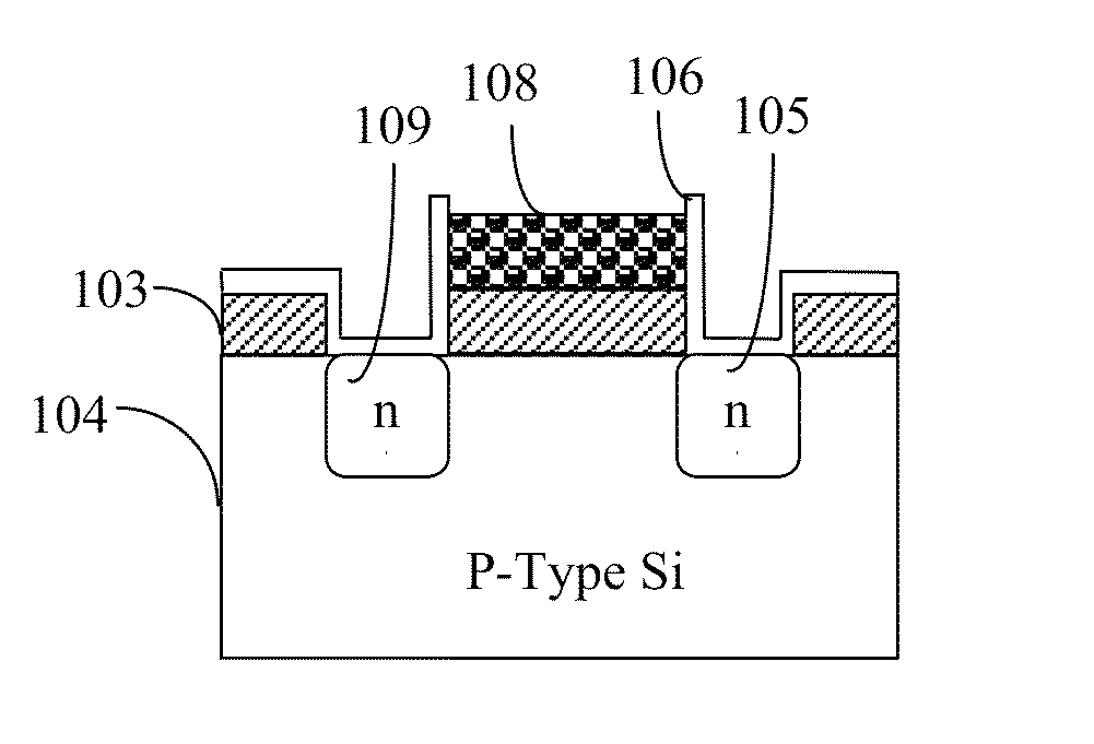
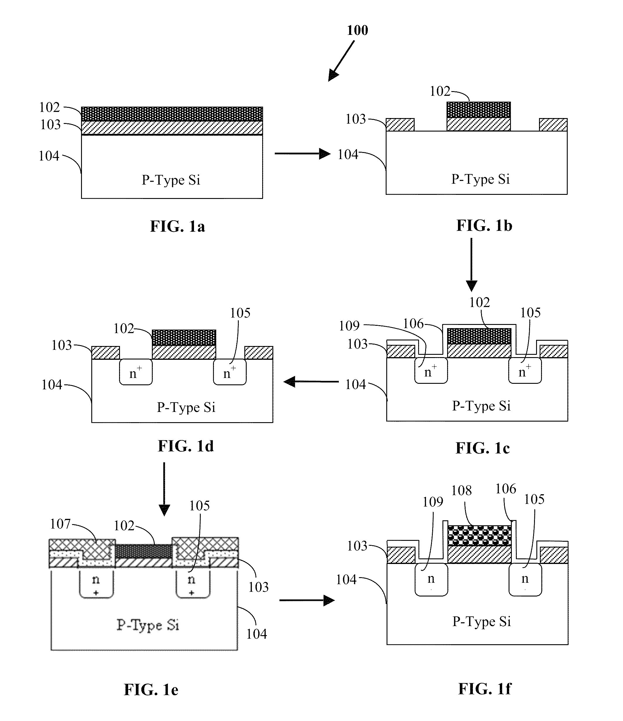
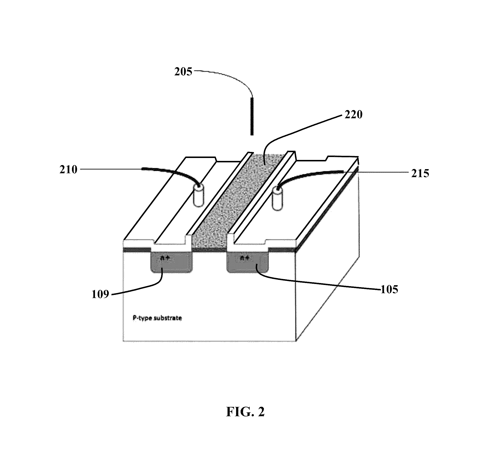
[0011]The primary object of the embodiments herein is to provide a method for fabricating gate region of an Ion-Selective Field-Effect Transistor (ISFET) with a nano porous layer.

[0012]Another object of the embodiments herein is to provide a method for fabricating the ISFET with a nano-porous layer to increase the effective adsorption surface of the ISFETs.

[0013]Yet another object of the embodiments herein is to provide a method for fabricating the ISFET with a nano-porous layer to make the nano-porous ISFET devices with an ultra high sensitivity due to a non-linear behavior.

[0014]Yet another object of the embodiments herein is to provide a method for fabricating the ISFET with a nano-porous layer adapted to act as an acceptor of biological objects when a physical adsorption is required.

[0015]Yet another object of the embodiments herein is to provide a method for fabricating the ISFET with a nano-porous layer to enhance the stabilization of one or more acceptors when a chemical adso...


PUM


Abstract

The various embodiments herein provide a method for fabricating Ion-Selective Field-Effect Transistor (ISFET) with a nano porous poly silicon layer on a gate region. The method includes providing a p-type silicon substrate and forming a silicon dioxide layer on the p-type silicon substrate. A poly silicon layer is deposited on the silicon dioxide layer. The poly silicon layer is patterned to form a gate region, a source region and a drain region in the silicon dioxide layer. A passivation layer is deposited on the gate region, source region and the drain region. The passivation layer is etched using a buffered HF to transform the poly silicon layer into a nano porous layer on the gate region by a sequential reactive ion etching process.

Description

[0001]This application claims the benefit of Provisional Application No. 61 / 472,283, filed on Apr. 6, 2011.BACKGROUND[0002]1. Technical Field[0003]The embodiments herein generally relate to Ion-Selective Field-Effect Transistors (ISFET) and particularly relate to highly sensitivity nano-porous ISFET devices. The embodiments herein more particularly relate to a fabrication of a high Ph sensitive ISFETs and a method for fabricating a gate region of the ISFET with a nano porous layer.[0004]2. Description of the Related Art[0005]Ion selective field effect transistors (ISFET) are microelectronic products that have an important role in the development of chemical sensors. ISFET is analogous to MOSFET transistors where the metallic gate is replaced by a sensitive membrane and a reference electrode. The silicon dioxide surface contains reactive SiOH groups that can be used for covalent attachment of organic molecules and polymers. The various characteristics of the ISFET such as rapid respo...

Claims


Application Information

Patent Timeline
Patent Type & Authority Patents(United States)
IPC IPC(8): H01L21/00
CPCG01N27/4148
Inventor MOHAJERZADEH, SHAMSODDINSHAHMOHAMMDI, MEHRANZEHFROOSH, NINA
Owner MOHAJERZADEH SHAMSODDIN
Features
  • R&D
  • Intellectual Property
  • Life Sciences
  • Materials
  • Tech Scout
  • Unparalleled Data Quality
  • Higher Quality Content
  • 60% Fewer Hallucinations
Learn More