Apparatus and methods for altering the timing of a clock signal

a clock signal and apparatus technology, applied in the field of apparatus and methods for altering the timing of clock signals, can solve problems such as significant jitter and problems in operation

Active Publication Date: 2014-02-04
MICRON TECH INC
View PDF13 Cites 33 Cited by
  • Summary
  • Abstract
  • Description
  • Claims
  • Application Information

AI Technical Summary

Problems solved by technology

Circuits in the clock path that include a chain of delay cells, for example, delay-lock loops, duty cycle correction circuits, and other delay circuits, may introduce significant jitter resulting from power supply variations because each delay cell may add a time variation.
Whereas the jitter introduced by each delay cell may not be significant, the sum of the time variations contributed by all of the delay cells may be enough to cause problems in operation.

Method used


Image

  • Apparatus and methods for altering the timing of a clock signal
  • Apparatus and methods for altering the timing of a clock signal
  • Apparatus and methods for altering the timing of a clock signal

Examples


Embodiment Construction

[0013]Certain details are set forth below to provide a sufficient understanding of embodiments of the invention. However, it will be clear to one skilled in the art that embodiments of the invention may be practiced without these particular details. Moreover, the particular embodiments of the present invention described herein are provided by way of example and should not be used to limit the scope of the invention to these particular embodiments. Various embodiments of circuits, devices, and systems according to the invention may be generally referred to as an apparatus or apparatuses. In other instances, well-known circuits, control signals, timing protocols, and software operations have not been shown in detail in order to avoid unnecessarily obscuring the invention.

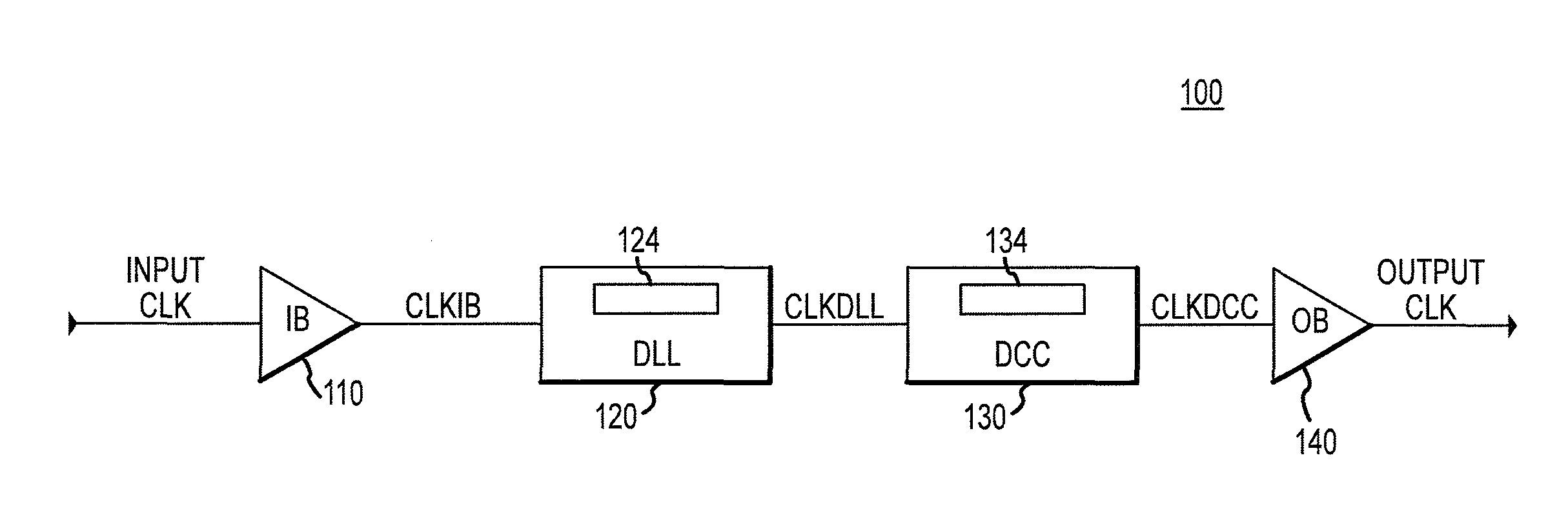
[0014]FIG. 1 illustrates a clock circuit 100 according to an embodiment of the invention. The clock circuit 100 includes an input buffer 110 configured to buffer an input clock signal INPUT CLK and provide a buffered ...


PUM


Abstract

Clock signal timing cells, clock signal timing circuits, clock circuits, memory devices, systems, and method for altering the timing of a clock signal are disclosed. An example method for altering the timing of an output signal provided responsive to an input clock signal includes adjusting a transition of an edge of the output signal from one voltage level to another based at least in part on a bias signal. An example clock signal timing cell includes an inverter and a bias controlled inverter coupled in parallel to the inverter. The bias controlled circuit is configured to provide an output signal wherein a transition of a clock edge of the output signal between first and second voltage levels is based at least in part on a bias signal.

Description

TECHNICAL FIELD[0001]Embodiments of the present invention relate generally to semiconductor memory and, more specifically, in one or more illustrated embodiments, to apparatus and methods for altering the timing of clock signals.BACKGROUND OF THE INVENTION[0002]Memory devices typically include a plurality of memory cells, which may be arranged in an array of intersecting rows and columns. Read and write operations, to respectively store and retrieve memory contents, may involve multiple steps and accessing multiple memory cells at approximately the same time. One or more clock signals can serve to synchronize activities in a memory device. Such clock signals can be distributed throughout the memory device through its clock distribution network. Various components of a clock path, for example clock drivers and delay cells of a delay line, can be sensitive to variations in supply voltage and / or current used to power the memory device. Clock path constituents can differ in their sensit...

Claims


Application Information

Patent Timeline
Patent Type & Authority Patents(United States)
IPC IPC(8): H03K5/12
CPCH03K19/00361H03K19/00369H03K5/01
Inventor MA, YANTAOWILLEY, AARON
Owner MICRON TECH INC
Why Eureka
Try Eureka