Method for post decomposition density balancing in integrated circuit layouts, related system and program product

a technology of density balancing and integrated circuits, applied in the field of integrated circuit design, layout, and fabrication, can solve the problems of inability to ensure that the desired patterning and electrical behavior are produced in the completed ic, difficulty in achieving density balancing, and prohibitively time-consuming to achieve density balancing using an automated decomposition tool

Active Publication Date: 2014-02-11
GLOBALFOUNDRIES US INC
View PDF8 Cites 32 Cited by
  • Summary
  • Abstract
  • Description
  • Claims
  • Application Information

AI Technical Summary

Problems solved by technology

However, with multiple patterning, the decomposition of a layout into e.g., two exposures by itself may not guarantee that the desired patterning and electrical behavior are produced in the completed IC.
This balance may be difficult to achieve during the design process, or manual decomposition, due to IC size and design processes which include the work of several individual IC designers whom are responsible for smaller sub-areas of the IC which may inadvertently conflict.
Further, it is also prohibitively time consuming to achieve density balancing using an automated decomposition tool, because of the need to solve a complex optimization problem on a large scale.
Conventional approaches of designing layouts for multiple patterning processes are deficient in producing the desired result.

Method used


Image

  • Method for post decomposition density balancing in integrated circuit layouts, related system and program product
  • Method for post decomposition density balancing in integrated circuit layouts, related system and program product
  • Method for post decomposition density balancing in integrated circuit layouts, related system and program product

Examples


Embodiment Construction

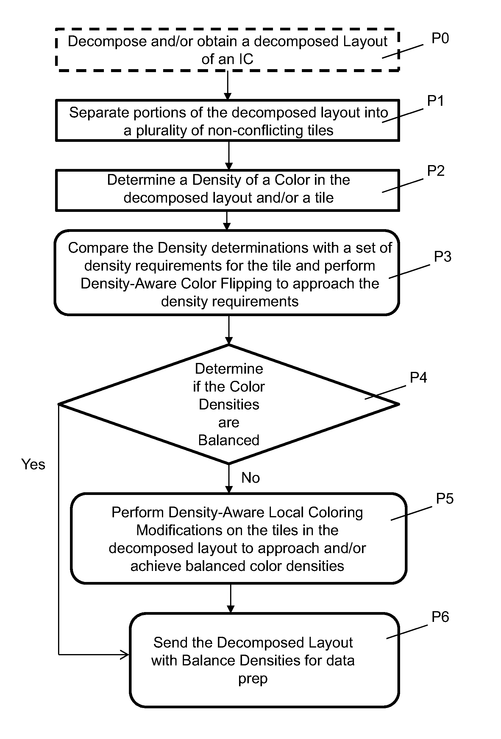
[0024]As noted, the subject matter disclosed herein relates to integrated circuits. More particularly, the subject matter relates to integrated circuit fabrication and layout design. These solutions are based on using color flipping and color modifications to balance densities on a decomposed layout, where the term “color” refers to a type of exposure mask. As used herein, different colors can refer to different types of exposure mask, e.g., red correlating with a first exposure mask, green correlating with second exposure mask, blue correlating with a third exposure mask, etc.

[0025]As described herein, in the case of multiple patterning, decomposing a layout into multiple (e.g., two exposures, three exposures, four exposures, etc.) exposures may not guarantee that the desired patterning is accurately produced in the completed IC. That is, it is also helpful to ensure that the density of shapes on both masks (in the double-patterning example) remains balanced, in order to ensure uni...


PUM


Abstract

Embodiments of the invention provide a method of modifying a decomposed integrated circuit (IC) layout. The method includes providing a decomposed IC layout, the decomposed IC layout including a set of colors; determining a density of each color in the decomposed IC layout, wherein each color includes a plurality of features formed by a related exposure; separating the decomposed IC layout into a set of tiles; determining a first color with a minimum density in one tile of the set of tiles and a second color with a maximum density in tile, the first color including a first set of first features and the second color including a first set of second features; and replacing the first set of second features on the tile with a second set of first features, and the first set of first features on the tile with a second set of second features.

Description

FIELD OF INVENTION[0001]The subject matter disclosed herein relates to integrated circuits. More particularly, the subject matter relates to integrated circuit design, layout, and fabrication.BACKGROUND[0002]As integrated circuit (IC) devices (also referred to as semiconductor devices) advance technologically, many designers and applications are calling for physically smaller ICs. Advanced patterning techniques have been developed in order to meet the design constraints associated with these smaller devices without sacrificing IC performance. For example, multiple patterning techniques, such as double patterning and / or triple patterning of masks and / or IC layers may be used to meet design constraints in smaller devices (e.g., at the 14 nanometer (nm) node, and potentially beyond this node). This multiple patterning allows for devices and features to be formed (e.g., printed) at a closer proximity relative to one another over the course of multiple prints. In multiple patterning, one...

Claims


Application Information

Patent Timeline
Patent Type & Authority Patents(United States)
IPC IPC(8): H01L21/66
CPCG05B19/41835G03F1/144G06F17/5081H01L22/12H01L2924/0002G06F30/398Y02P90/02H01L2924/00
Inventor AGARWAL, KANAK B.BANERJEE, SHAYAKLIEBMANN, LARS W.
Owner GLOBALFOUNDRIES US INC
Why Eureka
Try Eureka