Loaded printed circuit board test fixture and method for manufacturing the same

a printed circuit board and test fixture technology, applied in the field of test fixtures, can solve the problems of insufficient spring force for good electrical contact of spring probes suitable for fine pitch spacing on the probe plate, the inability to test high density test points on the printed circuit board, and the inability to manufacture the same, so as to achieve optimal manufacturing time and cost, good electrical contact

Active Publication Date: 2014-02-11
XCERRA
View PDF21 Cites 2 Cited by
  • Summary
  • Abstract
  • Description
  • Claims
  • Application Information

AI Technical Summary

Benefits of technology

[0011]A mechanical, pneumatic or vacuum pressure is applied to the test fixture, the high force spring probes apply force to the tilt pins in the translator fixture which is translated to the test points. The force translated from the high force spring probes provide good electrical contact between the tilt pins and the test points which is particularly important in the case of high density test points. The loaded board test fixture of the present invention further includes optimization software that provides the shortest interconnect distance in the x-y plane eliminating most, if not all of necessary manual wiring. The optimization software includes a translator pin mapping algorithm process which considers the property of the individual pins. Such properties would include, but not be limited to, analog signal, digital signal, power supply, ground, peripheral, ASRU, resistor termination, test jet, polarity check or any other discerning characteristic. The optimization software also calculates the position of the loaded board location and rotation on the top of the translator fixture for optimal manufacturing time and cost with respect to the properties of the translator pins. The optimization software further includes a sizing algorithm which determines the optimal pin diameter and length based upon application, pin angle and loaded board contact characteristics.

Problems solved by technology

In these grid type testers, fixturing is generally less complex and simpler than the customized wired test fixtures because there is no need to individually hard wire the test probes to separate interface contacts for each differently configured circuit to be tested; but with a grid system, the grid interfaces and test electronics are substantially more complex and costly.
A problem encountered with these types of fixtures for testing loaded circuit boards is the ability to test high density test points on the printed circuit board.
However, spring probes suitable for fine pitch spacing on the probe plate do not have a spring force sufficient to provide good electrical contact with the test points on the PCB.

Method used


Image

  • Loaded printed circuit board test fixture and method for manufacturing the same
  • Loaded printed circuit board test fixture and method for manufacturing the same
  • Loaded printed circuit board test fixture and method for manufacturing the same

Examples


Embodiment Construction

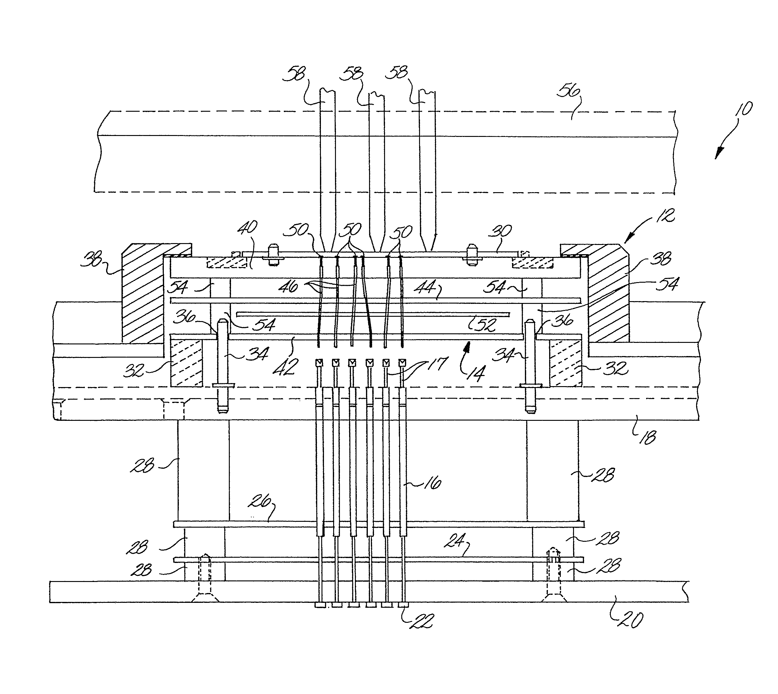
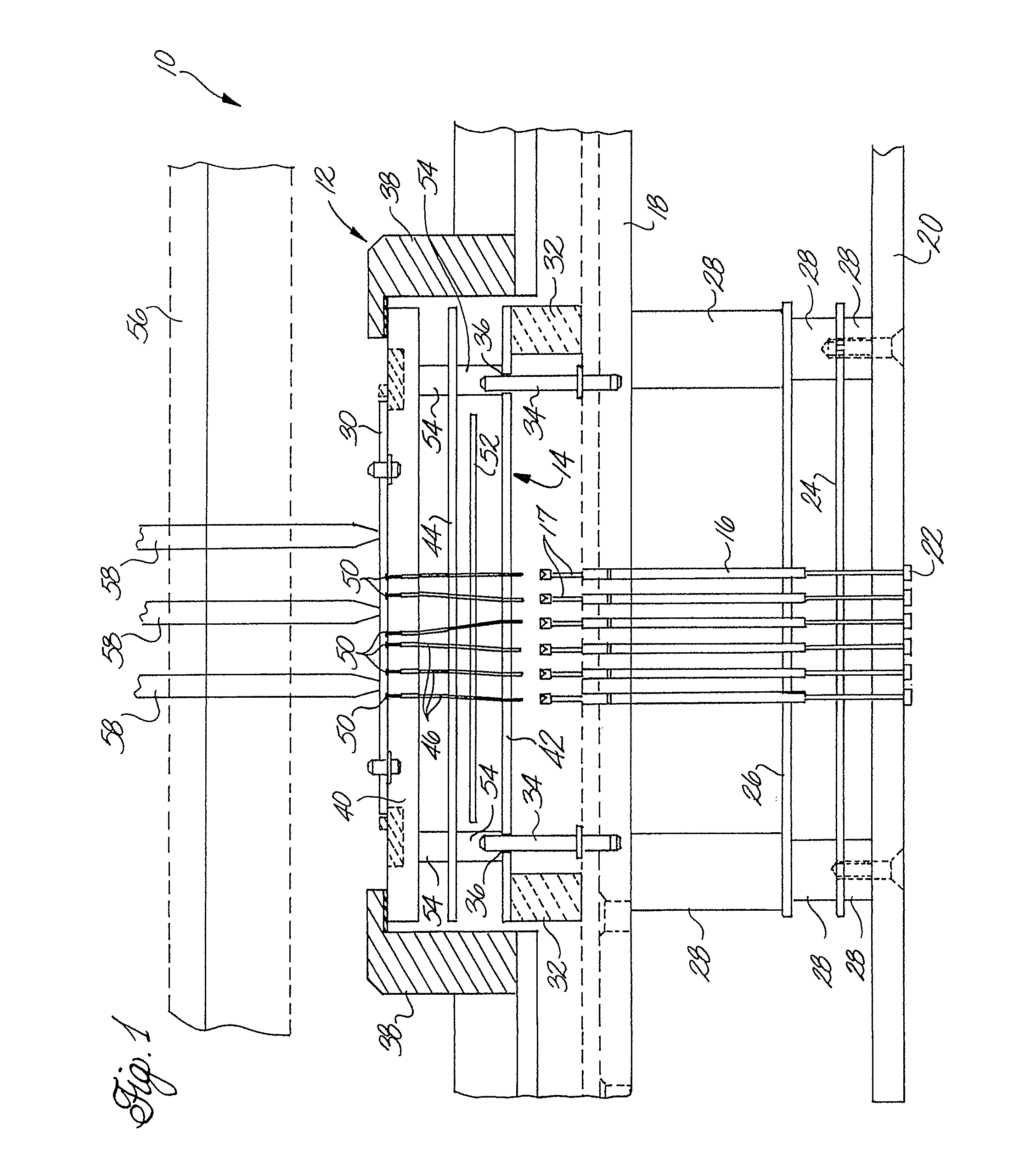
[0024]FIG. 1 illustrates a loaded board test fixture 10 in accordance with the principals of this invention. The test fixture is principally used to align a printed circuit board in a test position for use with an electronic test analyzer. The invention is particularly useful in the testing of loaded circuit boards as distinguished from bare boards. In one example, the test fixture 10 comprises a vacuum test fixture 12 and a translator fixture 14 removably positioned within the vacuum fixture. The vacuum fixture includes a plurality of electronically conductive spring probes 16 positioned in corresponding holes in a non-conductive upper probe plate 18 located in the fixture. The spring probes are arranged in a hole pattern sufficiently far apart to accommodate spring probes, preferably spaced apart 100 mils on center. The 100 mils spring probes should be able to deliver a sufficient spring force in a range from about 4 to about 16 ounces. Typical 100 mil spring probes are made from ...


PUM


Abstract

A test fixture for testing loaded printed circuit boards having a plurality of test points having a probe plate including an array of widely spaced high force spring test probes in compliant contact with solid translator pins located in a translator fixture removably positioned over the probe plate. The test fixture includes optimization software wherein translation of the test signals are optimized by providing the shortest interconnect distance in the x-y plane between the test points on the printed circuit board and the test probes in the probe plate. The fixture further includes an unpowered opens device for testing components on the loaded printed circuit board.

Description

CROSS-REFERENCE TO RELATED APPLICATION(S)[0001]This application claims priority to U.S. Provisional Application No. 61 / 289,339 filed Dec. 22, 2009, the contents thereof are incorporated herein.BACKGROUND OF THE INVENTION[0002]This invention relates to test fixtures for the automatic testing of loaded printed circuit boards, and more particularly to a test fixture utilizing a tilt pin translating fixture that contains an optimized translation for the test probes for testing high pitch density test patterns.[0003]Automatic test equipment for checking printed circuit boards has long involved the use of a “bed-of-nails” test fixture to which the circuit board is mounted during testing. This test fixture includes a large number of nail-like, spring loaded test probes arranged to make electrical contact under spring pressure with designated test points on the circuit board under test (UUT). Any particular circuit laid out on a printed circuit board (PCB) is likely to be different from oth...

Claims


Application Information

Patent Timeline
Patent Type & Authority Patents(United States)
IPC IPC(8): G01R1/067
CPCG01R31/31905G01R1/07328G01R1/07378
Inventor ST. ONGE, GARY F.GOLD, SCOTT F.MICZEK, MATTHEW T.
Owner XCERRA
Why Eureka
Try Eureka