

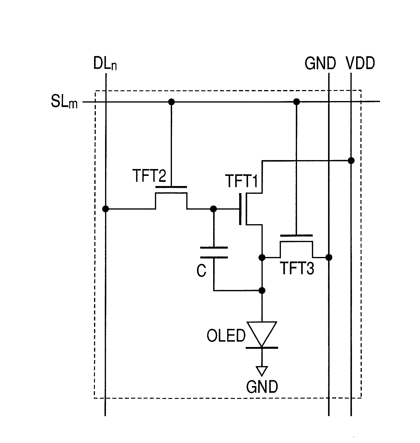
Thin film transistor circuit, light emitting display apparatus, and driving method thereof
a technology of light-emitting display and thin film transistor, which is applied in the direction of oscillator, pulse technique, instruments, etc., can solve the problems of above problem (3) and still remain, and achieve the effect of suppressing the deterioration of display quality
- Summary
- Abstract
- Description
- Claims
- Application Information
AI Technical Summary
Benefits of technology
Problems solved by technology
Method used
Image

Examples
embodiment 1
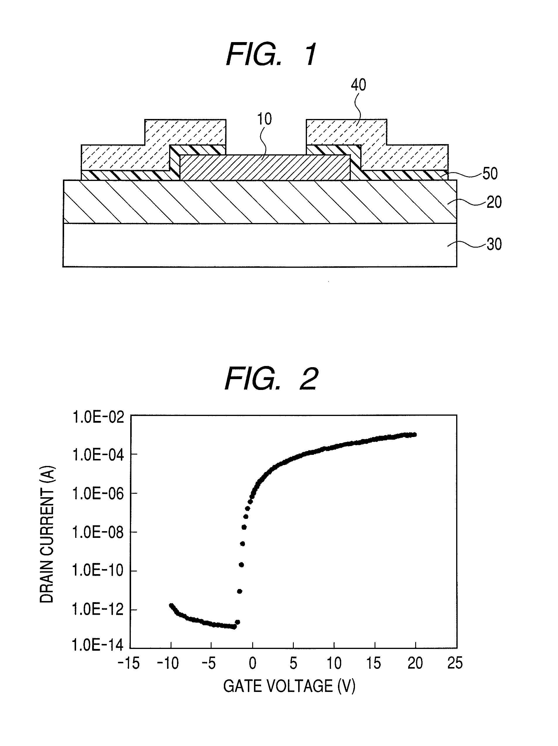
[0038]First, the characteristic of a TFT, in which the a-IGZO to be used in the present embodiment is treated as a channel layer, will be described.
[0039]A fabricating method of the a-IGZO TFT will be indicated as below.
[0040]As indicated in FIG. 1, a thermally-oxidized SiO2 insulation film 20, of which thickness is 100 nm, is formed on an Si substrate 30, to which impurity such as P (phosphorus) or As (arsenic) is densely injected. Here, a part of the Si substrate 30 constitutes a gate electrode.
[0041]Thereafter, an a-IGZO film 10, of which thickness is 50 nm, is deposited in the room temperature by a sputter deposition method by treating a polycrystalline IGZO as a target. Next, a channel layer is formed by patterning the a-IGZO film 10 by a wet etching process depending on a photolithography method and the dilute hydrochloric acid.
[0042]Subsequently, after depositing a Ti payer (5 nm) 50 and an Au layer (40 nm) 40 by an EB (electron beam) vapor deposition method upon patterning t...
embodiment 2
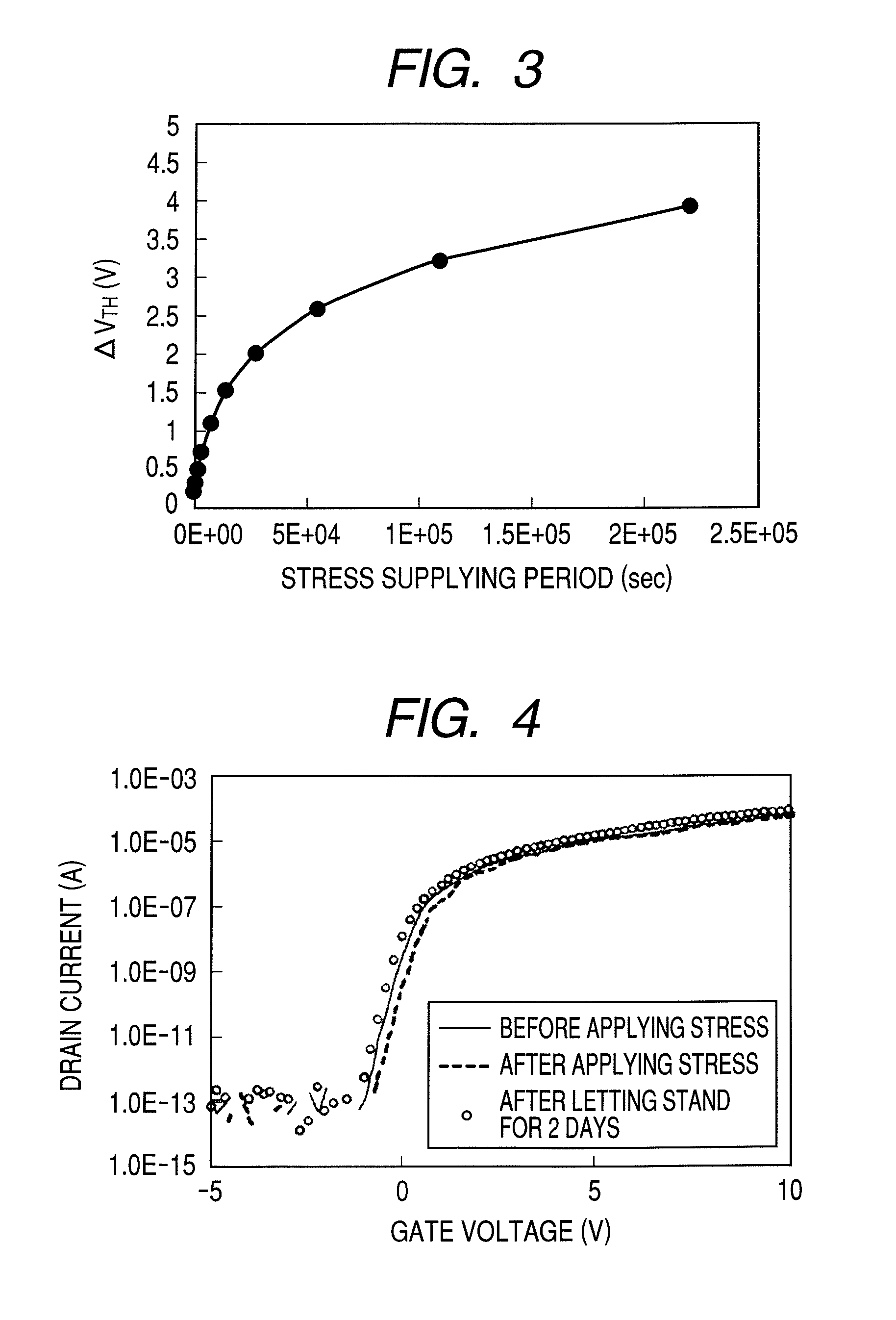
[0078]An organic EL display apparatus of the present embodiment further includes a battery in the organic EL display apparatus of the Embodiment 1, and an operation of applying the electrical stress is enabled to be performed in at least a part of the non-displaying period indicated in the Embodiment 1 without supplying the power from an external.
[0079]After completing to fabricate the product, the TFT1 can be realized to operate in the saturated region of the threshold voltage for the electrical stress by applying the electrical stress. Additionally, the TFT1 can be kept in a state of operating in a region that the change for the electrical stress is saturated until a time before starting to use by performing an operation in the above-described non-display state by using the battery.
[0080]Furthermore, by providing the battery, the TFT1 can be kept in a state of operating in the region that the change for the electrical stress is saturated even if in a case that the organic EL displ...
PUM
 Abstract
Description
Claims
Application Information