Organic electroluminescence element, display device using organic electroluminescence element, and method of manufacturing organic electroluminescence element

a technology of organic electroluminescence and display device, which is applied in the direction of organic semiconductor devices, thermoelectric devices, solid-state devices, etc., can solve the problems of insufficient tolerance, inability to achieve satisfactory combinations of first and second metal compounds in some cases, and inability to achieve satisfactory combinations of first and second metal compounds. achieve high luminance luminescence, long lifetime, and high efficiency

Inactive Publication Date: 2014-03-18
TOPPAN PRINTING CO LTD
View PDF17 Cites 0 Cited by
  • Summary
  • Abstract
  • Description
  • Claims
  • Application Information

AI Technical Summary

Benefits of technology

[0037]The invention is devised in the light of the above-mentioned circumstance and an object of the invention is to provide a method of manufacturing an organic EL element that has environmental tolerance or solvent tolerance by the use of a metal compound mixed film in various manufacturing processes or combinations of layers adjacent to the metal compound mixed film and has compatibility between the characteristics of high efficient luminescence, high luminance luminescence, and long lifetime. Further, another object of the invention is to provide an EL element and a method of manufacturing a display device that has the characteristics of high efficient luminescence, high luminance luminescence, and long lifetime obtained by the use of a normal metal compound mixed film.

Problems solved by technology

However, combinations of first and second metal compounds are quite restrictive due to the compatibility between various matter properties including a work function of a metal compound mixed film and layers adjacent to the metal compound mixed film.
However, the satisfactory combinations of the first and second metal compounds may not be realized in some cases, for example, when sufficient luminescent characteristics may not be obtained or when the luminescent characteristics are satisfactory but sufficient tolerances may not be obtained.

Method used


Image

  • Organic electroluminescence element, display device using organic electroluminescence element, and method of manufacturing organic electroluminescence element
  • Organic electroluminescence element, display device using organic electroluminescence element, and method of manufacturing organic electroluminescence element
  • Organic electroluminescence element, display device using organic electroluminescence element, and method of manufacturing organic electroluminescence element

Examples


example 1

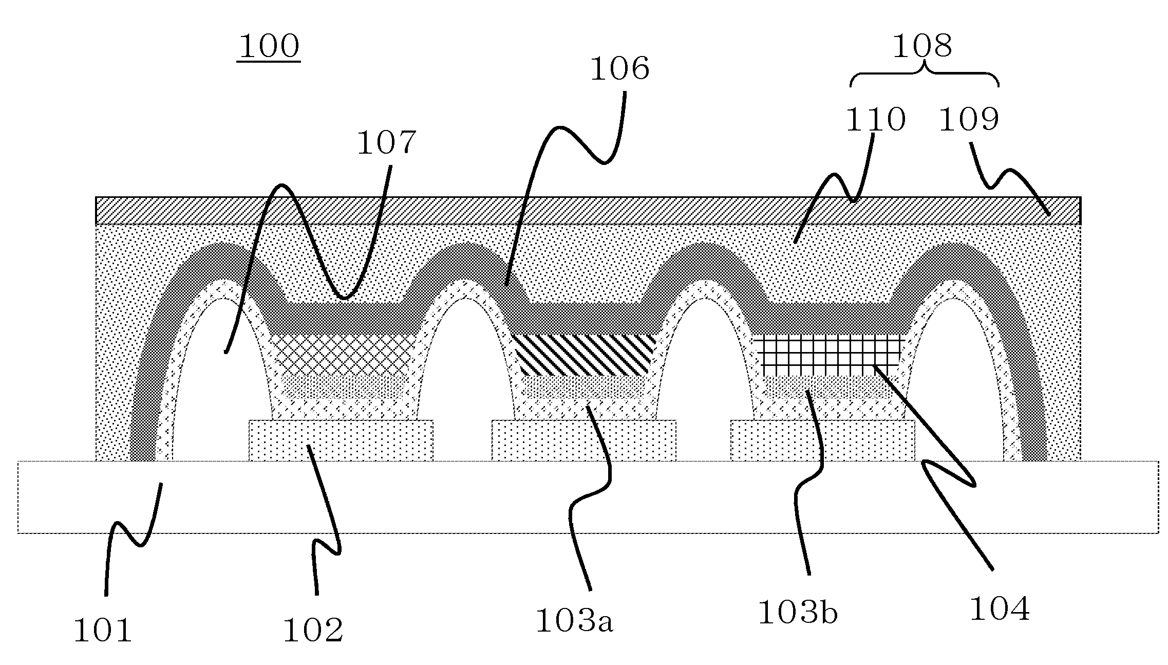
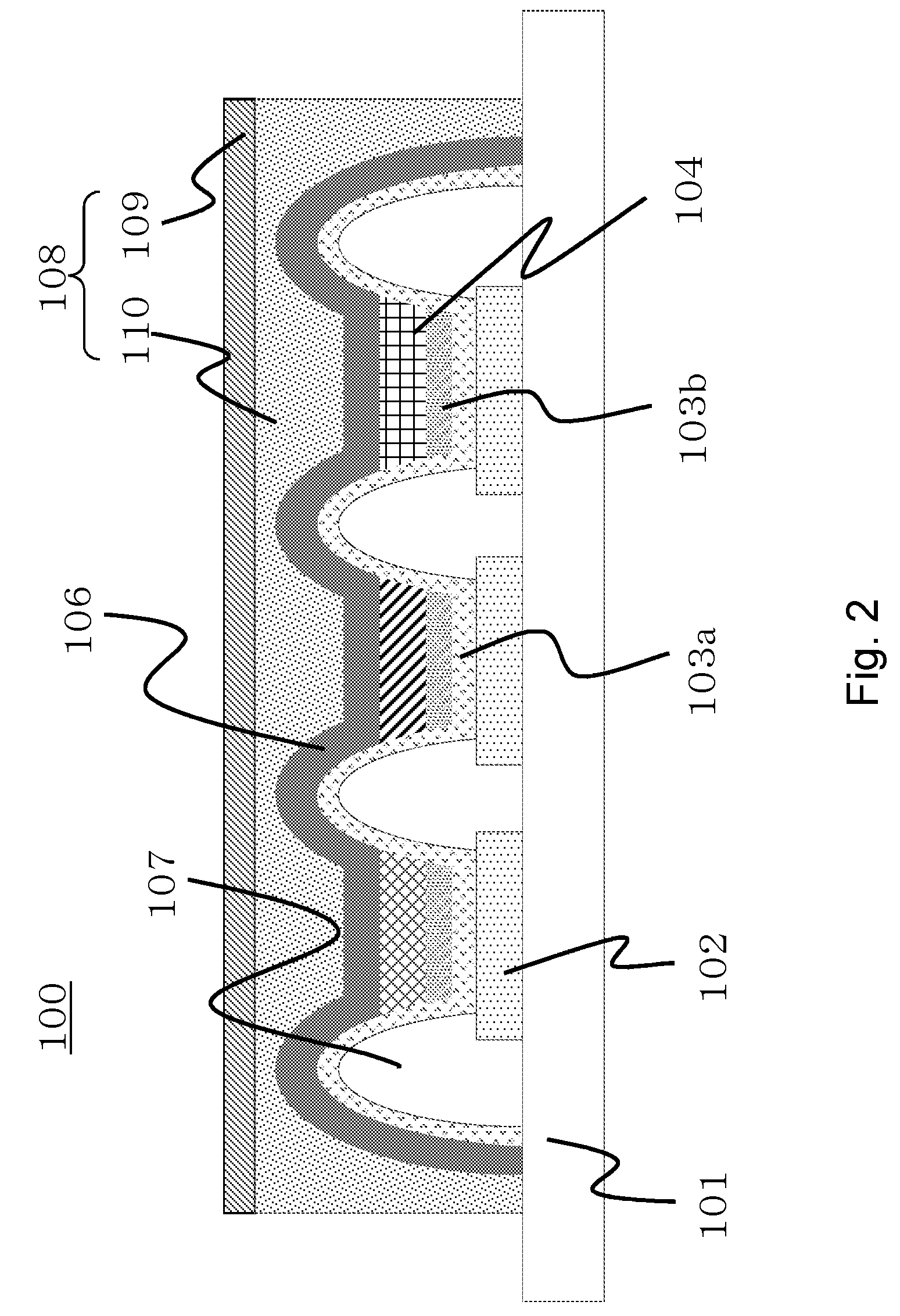
[0129]First, a glass substrate is used as the substrate. ITO as a material of the anode was formed on the substrate in a vacuum by a sputtering method and the ITO film was patterned by a photolithography method and etching of an acid solution to form a luminescent electrode section.

[0130]Next, an acrylic-based photoresist material was spin-coated as the material of an insulation layer on the entire surface of the glass substrate on which the luminescent electrode section was formed. As the condition of the spin coating, the acrylic-based photoresist material was rotated for five seconds at 150 rpm, and then was for twenty seconds at 500 rpm to obtain a conductive film with a height of 1.5 μm. Thereafter, a pattern with a lattice shape was formed by a photolithography method on the luminescent electrode section.

[0131]Next, molybdenum oxide and titanium oxide were co-deposition as the hole-injection layer and the hole-carrying layer in a vacuum and the deposition speed of the titanium...

example 2

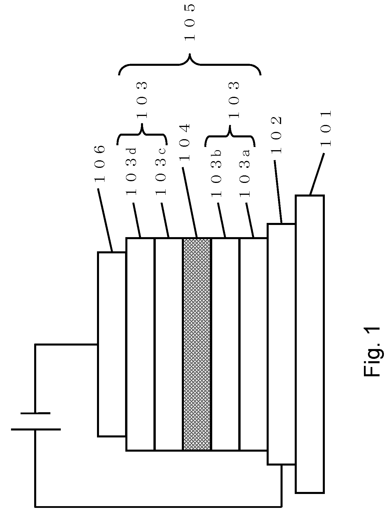
[0136]An element was manufactured by the use of the same method and material as those of Example 1. At this time, the mixture gradient film was formed with a gradient so that the concentration of titanium oxide was 66 wt % on the side of the anode and was 0 wt % on the side of the cathode. The mixture ratio of the mixture gradient film was obtained with the gradient shown in the right lower side of FIG. 10.

[0137]The luminescent of the formed organic EL element was good without irregularity or a dark spot. The luminance at 7 V was 1360 cd / m2 and a luminance half-life time at initial luminance of 1500 cd / m2 was 290 hours, and thus the element characteristics of low-voltage driving, high luminance, and long lifetime were obtained. Further, a defect such as a dark spot was not recognized at an acceleration experiment.

example 3

[0138]An element was manufactured by the use of the same method and material as those of Example 1. At this time, the mixture gradient film was formed with a gradient so that the concentration of titanium oxide was 12 wt % on the side of the anode and was 62 wt % on the side of the cathode. The mixture ratio of the mixture gradient film was obtained with the gradient shown in FIG. 6.

[0139]The luminescent of the formed organic EL element was good without irregularity or a dark spot. The luminance at 7 V was 1280 cd / m2 and a luminance half-life time at initial luminance of 1500 cd / m2 was 325 hours, and thus the element characteristics of low-voltage driving, high luminance, and long lifetime were obtained. Further, a defect such as a dark spot was not recognized at an acceleration experiment.


PUM

PropertyMeasurementUnit
thicknessaaaaaaaaaa
thicknessaaaaaaaaaa
thicknessaaaaaaaaaa

Abstract

One embodiment of the present invention is an organic electroluminescence element including: a substrate; a first electrode that is formed on the substrate; a luminescent medium layer that includes at least an organic luminescent layer and one or more functional layers other than the organic luminescent layer formed on the first electrode; and a second electrode that faces the first electrode with the luminescent medium layer interposed therebetween, wherein at least one functional layer formed between the first electrode and the organic luminescent layer includes first and second metal compounds and the functional layer is a functional layer in which a gradient is obtained at least partially in a film thickness direction for a ratio of the first metal compound to the second metal compound.

Description

CROSS REFERENCE TO RELATED APPLICATION[0001]This application is a continuation of International Application No. PCT / JP2010 / 065874, filed Sep. 14, 2010, the entire contents of which is incorporated herein by reference.[0002]This application is based upon and claims the benefit of priority from the prior Japanese Patent Application No. 2009-226859, filed on Sep. 30, 2009, the entire content of which is incorporated herein by reference.BACKGROUND OF THE INVENTION[0003]1. Field of the Invention[0004]The invention relates to an organic electroluminescence element (hereinafter, referred to as an organic EL element), a display device including the organic EL element, and a method of manufacturing the organic EL element.[0005]2. Background Art[0006]An organic EL element has a configuration in which an organic luminescent layer showing at least an electroluminescence phenomenon is interposed between an electrode as an anode and an electrode as a cathode. The organic EL element is a spontaneo...

Claims


Application Information

Patent Timeline
Patent Type & Authority Patents(United States)
IPC IPC(8): H01L29/12H01L29/08
CPCH01L2251/308H01L51/0038H01L51/5088H01L2251/5346H10K85/114H10K50/17H10K2101/80H10K2102/103
Inventor OKAMOTO, SHINICHISHODA, RYO
Owner TOPPAN PRINTING CO LTD
Why Eureka
Try Eureka