Luminescent Device and Display Device Using Same

a technology of luminescent devices and display devices, which is applied in the direction of luminescent compositions, organic semiconductor devices, luminescent compositions, etc., can solve the problems of low luminescence efficiency, high turn on voltage, and poor device performance of such devices

Inactive Publication Date: 2019-04-18
AAC TECH PTE LTD
View PDF4 Cites 2 Cited by
  • Summary
  • Abstract
  • Description
  • Claims
  • Application Information

AI Technical Summary

Problems solved by technology

The device performance of such device structure is very poor, for example, the turn on voltage needs 14V.
This is because, in general, the HOMO and LUMO of the luminescent material are very mismatched with the anode or cathode, resulting in difficulties in the hole or electron injection, and therefore, a very high turn on voltage is required.
In the electroluminescence process, the exciton concentration of the luminescence is very high, which leads to the quenching of the exciton, resulting in very low luminescence efficiency.
(1) ΔE is much larger than 0. The host material energy level T1,H is much larger than the guest material's energy level T1,G, and even the KF is much larger than KR, so that both cannot produce energy resonance, therefore, in the process of electroluminescence, the energy formed on the host material cannot be effectively transferred to the host material for efficient luminescence.
(2) ΔE>0. This is the most ideal energy transfer system. In this device structure KF>KR, there is an effective energy resonance between the host material and the guest material, so a good host and guest energy transfer process can take place.
The concentration quenching of excitons in the luminescent layer is an important factor to reduce the performance of OLED devices.
However, whether phosphorescence OLED or fluorescence OLED, too much exciton density (doping concentration is too high) will often lead to the above phenomenon, but if the doping concentration is reduced, the energy transfer between host and guest will be incomplete, and the device efficiency will also be reduced.
This will increase the complexity of the OLED manufacturing process and increase the production costs.

Method used


Image

  • Luminescent Device and Display Device Using Same
  • Luminescent Device and Display Device Using Same
  • Luminescent Device and Display Device Using Same

Examples


embodiment 1

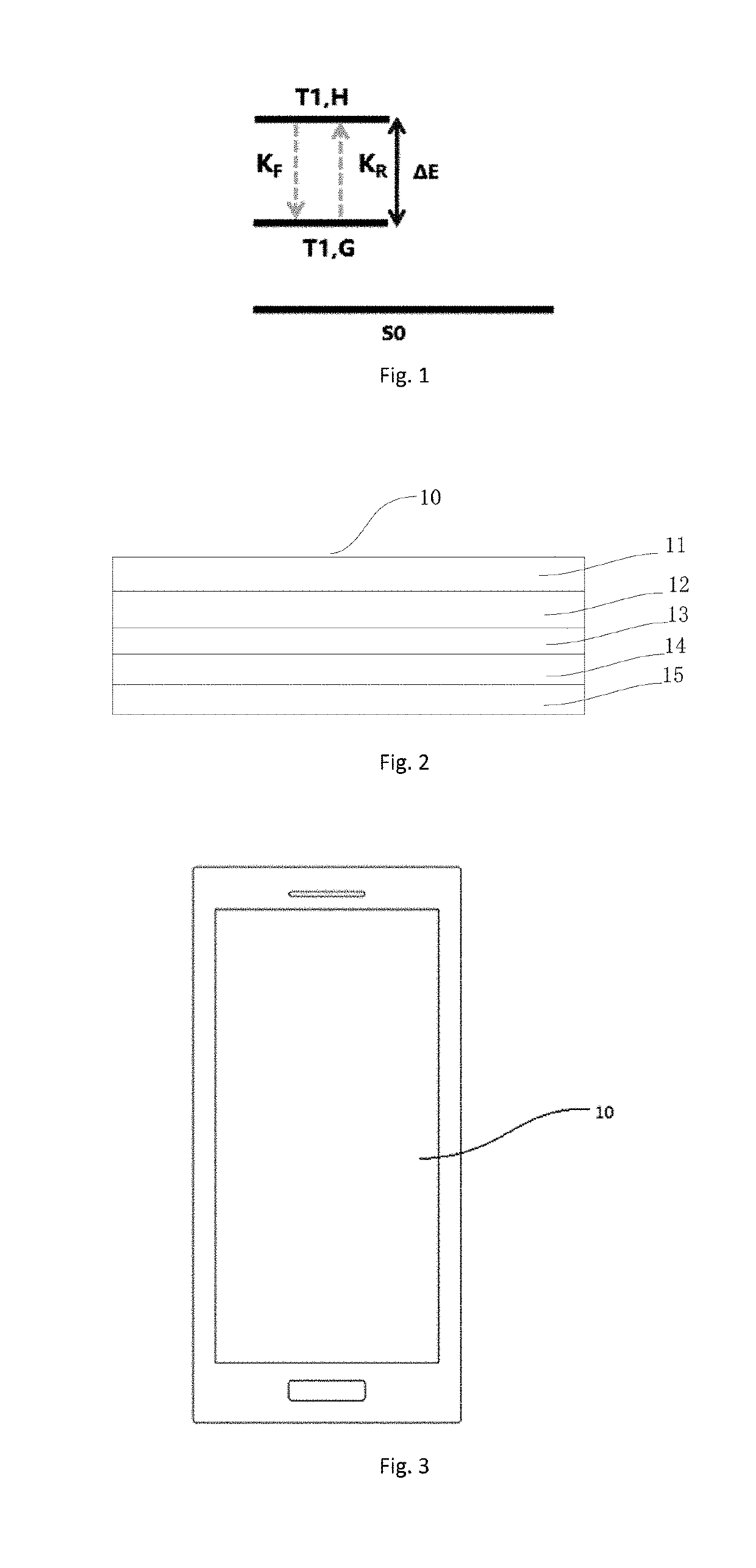
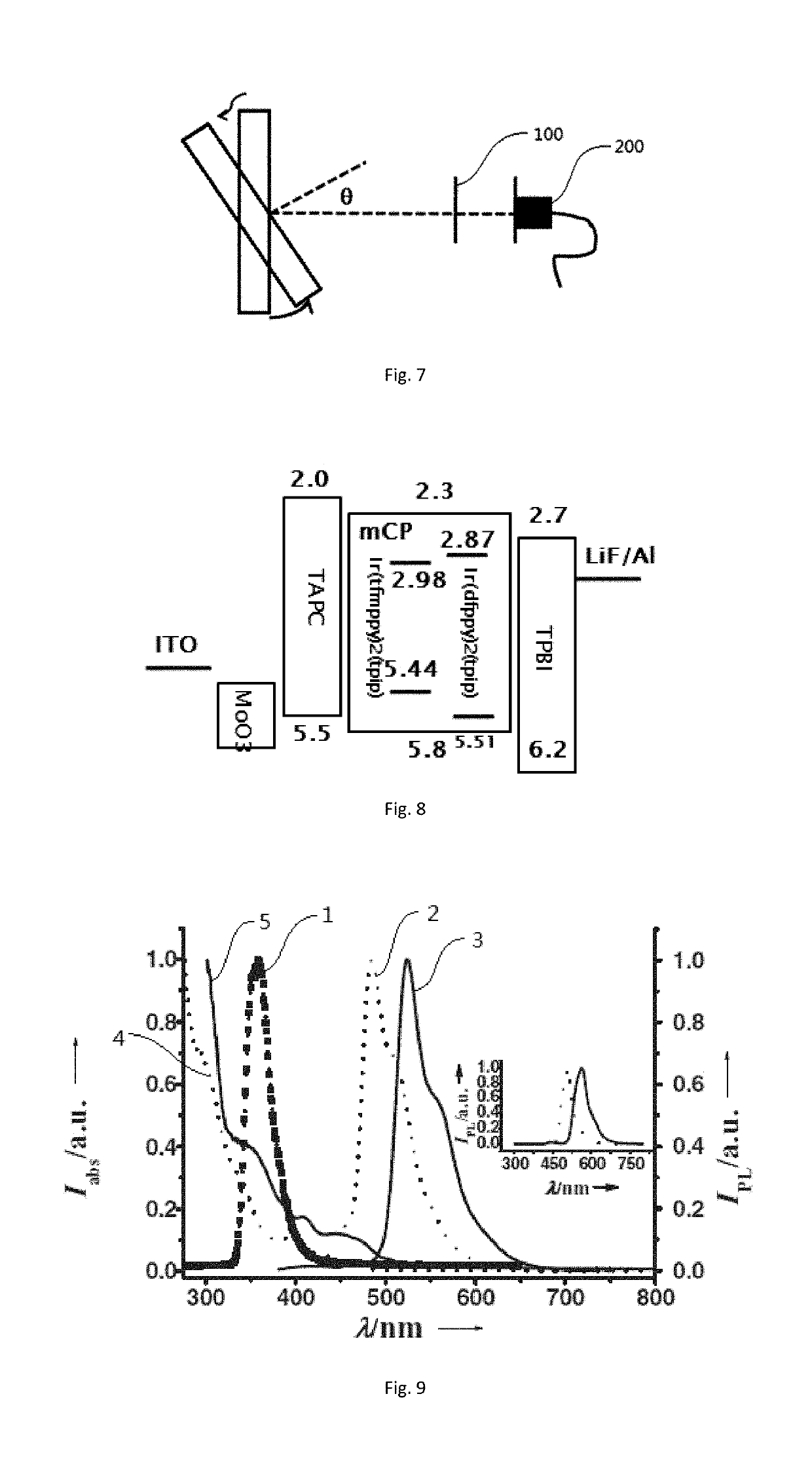
[0093]To construct the multilayer device structure of ITO / HIL / HTL / step photoluminescence layer / ETL / EIL / cathode, the chemical structure of some organic materials is as follows:

[0094]Among them, MoO3 is used as a hole injection layer material, TAPC is used as a hole transport layer material, and mCP is used as a host material. Ir(dfppy)2 / (tpip) is used as an energy level transition layer material, and a doping amount is 15 wt. %, Ir(tfmppy)2 / (tpip) is used as a green light oriented guest material, and a doping amount is 5 wt. %. TPBI is used as an electron transport layer and a hole barrier material, and LiF is as an electron injection layer material and Al is used as a cathode. Ir(tfmppy)2(tpip) is a heterocyclic ligand metal chelate with large vertical transition dipole moment DVT that can be used as a light-oriented guest material.

[0095]Analysis of energy level and spectral characteristics:

[0096]The triplet energy level of TAPC T=2.87 eV, and the triplet energy level of TPBi T1=2.7...

embodiment 2

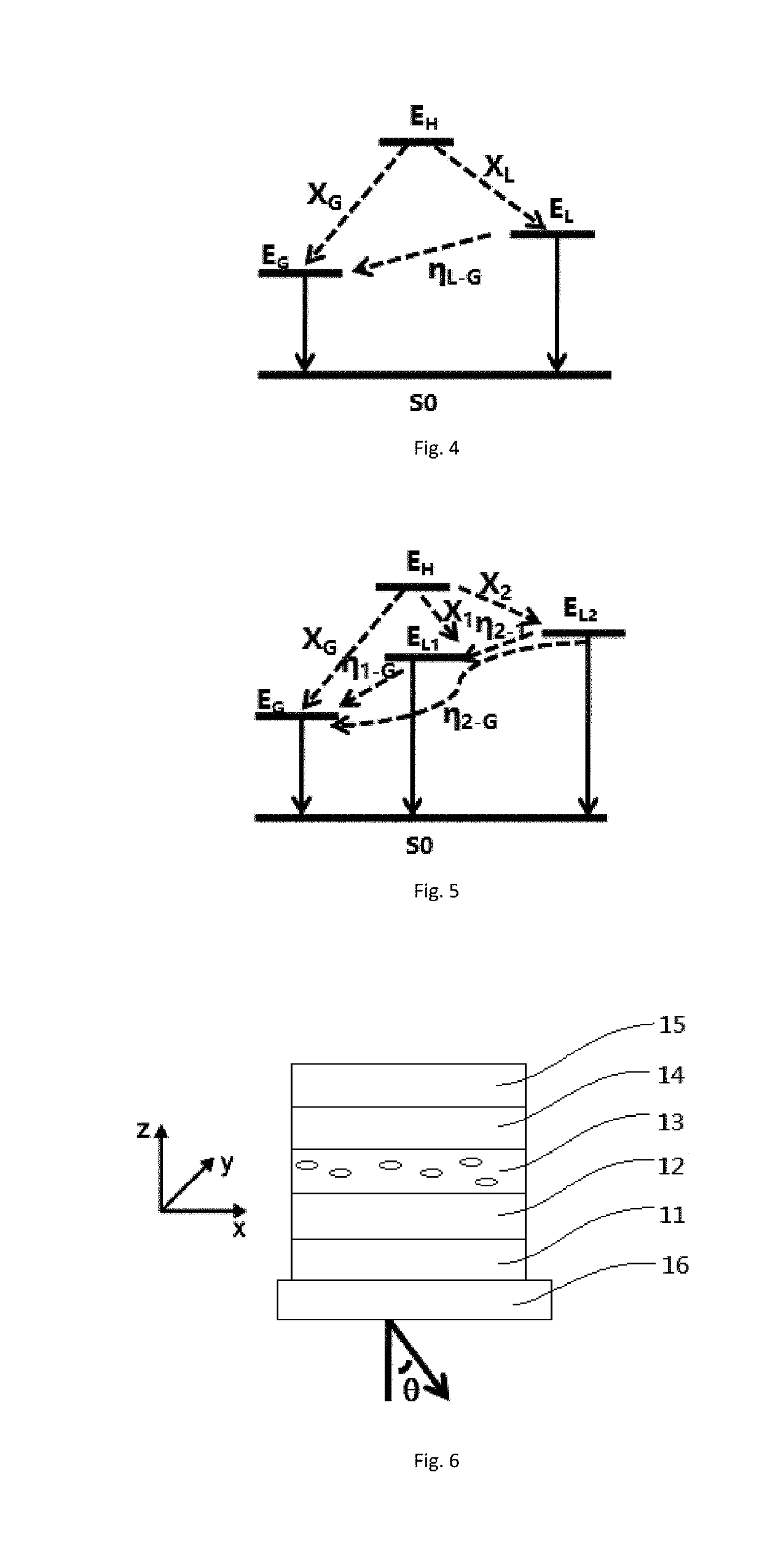
[0119]The multilayer device structure of ITO / HIL / HTL / step light-oriented photoluminescence layer and ETL / EIL / cathode is constructed. The chemical structure of some of the organic materials used is as follows:

[0120]In green or yellowish-green devices, mCP is used as the host material, FIrpic is used as the transition layer material, and the green or yellow light light-oriented guest materials are taken from Ir(ppy)3, Ir(ppy)2(acac), Ir(bppo)2(acac), Ir(chpy)3, Ir(bppo)2(ppy). The properties of the light-oriented guest materials are shown in Table 1.

[0121]Analysis of energy level and spectral characteristics:

[0122]The triplet energy level of the host material mCP T1=2.9 eV;

[0123]The triplet energy levels of the energy level transition layer FIrpic are higher than T1 energy level of green or yellowish-green light oriented guest materials (as shown in Table 1).

[0124]According to the spectral data of the above host material, the energy level transition layer material and the light-orient...

embodiment 3

[0137]The multilayer device structure of ITO / HIl / HTL / step photoluminescence layer and ETL / EIL / cathode is constructed. The chemical structure of some organic materials used is as follows:

[0138]The red light device uses CBP as the host material, and Ir(ppy)3 as the energy level transition layer. The red light-oriented guest material is obtained from Ir(MDQ)2(acac), Ir(ppy)2(bppo), Ir(piq)3. The properties of the light-oriented guest materials are shown in Table 1.

[0139]Analysis of energy level and spectral characteristics:

[0140]The triplet energy levels of the host material CBP and the transition layer Ir(ppy)3 are higher than the T1 energy level of the red light-oriented guest material.

[0141]In order to further investigate the energy transfer efficiency of the host material, the energy level transition layer material and the light-oriented guest material in the luminescent layer, the spectral information of the three materials is as follows:

[0142](1) The photoluminescence spectra of ...


PUM

PropertyMeasurementUnit
luminescentaaaaaaaaaa
energy levelaaaaaaaaaa
energyaaaaaaaaaa

Abstract

The invention relates to the field of organic luminescent technology, in particular to a luminescent device and a display device. The luminescent device includes a first electrode, a second electrode and at least a luminescent layer arranged between the first electrode and the second electrode. The luminescent layer includes at least a host material, at least an energy level transition layer material and at least a guest material; the energy level transition layer material can receive the energy of the host material and transfer the energy to the guest material, thus solving the problem where the energy formed on the host material cannot be effectively transferred to the guest material to carry on the high efficiency luminescence during electroluminescence when the difference between the host material T1 energy and the guest material T1 energy is large, in order to greatly improve the efficiency of the luminescent device.

Description

FIELD OF THE PRESENT DISCLOSURE[0001]The invention relates to the field of organic luminescent technology, in particular to a luminescent device and a display device thereof.DESCRIPTION OF RELATED ART[0002]A luminescent device—Organic Light-Emitting Diode (OLED) comes into being and gradually enters the field of vision as a new generation of flat panel display technology. OLED is characterized by its own luminescence, unlike the thin-film transistor liquid crystal display (TFT-LCD), which requires backlight, so it has high visibility and brightness, followed by low voltage demand and high power saving efficiency. Coupled with fast reaction, light weight, thin thickness, simple construction and low cost etc, it is regarded as one of the most promising products in 21th century. At present, in the application of mobile phone screen, OLED replacing Liquid Crystal Display (LCD) has become the trend of the times. Some Samsung models of cell phones already use the OLED screen, and Apple Co...

Claims


Application Information

Patent Timeline
Patent Type & Authority Applications(United States)
IPC IPC(8): H01L51/50H01L51/56H01L51/00C09K11/06
CPCH01L51/5028H01L51/5004H01L51/5016H01L51/56H01L51/001C09K11/06H01L2251/552H01L51/0059H01L51/0072C09K2211/185C09K2211/1029H01L51/0085H10K85/623H10K85/624H10K50/11H10K2101/40H10K71/00H10K85/342H10K50/121H10K71/164H10K85/631H10K85/6572H10K2101/10H10K2101/30
Inventor XIE, ZAIFENG
Owner AAC TECH PTE LTD
Why Eureka
Try Eureka