
Method of manufacturing semiconductor device

a manufacturing method and semiconductor technology, applied in the direction of semiconductor devices, electrical devices, transistors, etc., can solve the problem of difficult to suppress the growth of nisisub>2 /sub>crystals in spikes

Inactive Publication Date: 2014-03-25
FUJITSU SEMICON LTD
View PDF41 Cites 2 Cited by
  • Summary
  • Abstract
  • Description
  • Claims
  • Application Information

AI Technical Summary

Benefits of technology

This approach effectively prevents platinum residue formation, reduces contact resistance, and suppresses the growth of nickel disilicide crystals in spikes, improving the characteristics and reliability of semiconductor transistors, especially at small gate widths.

Problems solved by technology

Even in using a Ni alloy film, such as a NiPt film or others, for the silicidation, it is often difficult to suppress the growth of the NiSi2 crystals in spikes.

Method used


Image

  • Method of manufacturing semiconductor device
  • Method of manufacturing semiconductor device
  • Method of manufacturing semiconductor device

Examples


first embodiment

A First Embodiment

[0075]Before the method of manufacturing the semiconductor device according to the present invention is explained, the silicidation process using a nickel platinum (NiPt) film will be explained with reference to FIGS. 47A-47C, 48A-48B and 49A-49C.

[0076]FIGS. 47A-48C and 48A-48B are sectional views showing the steps of a proposed method of manufacturing a semiconductor device (Part 1).

[0077]First, on a silicon substrate 200, a MOS transistor 216 including a gate electrode 206 and source / drain diffused layers 214 is formed by the usual MOS transistor manufacturing method.

[0078]FIG. 47A illustrates the MOS transistor formed on the silicon substrate 200. As illustrated, a device region is defined by a device isolation region 202 on the semiconductor substrate 200. On the silicon substrate 200 with the device region defined, the gate electrode 206 of a polysilicon film is formed with a gate insulating film 204 formed therebetween. A sidewall insulating film 208 is forme...

second embodiment

A Second Embodiment

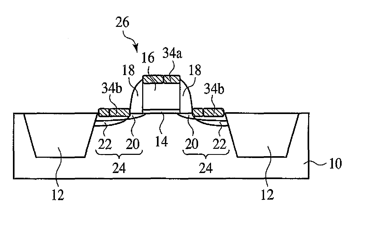
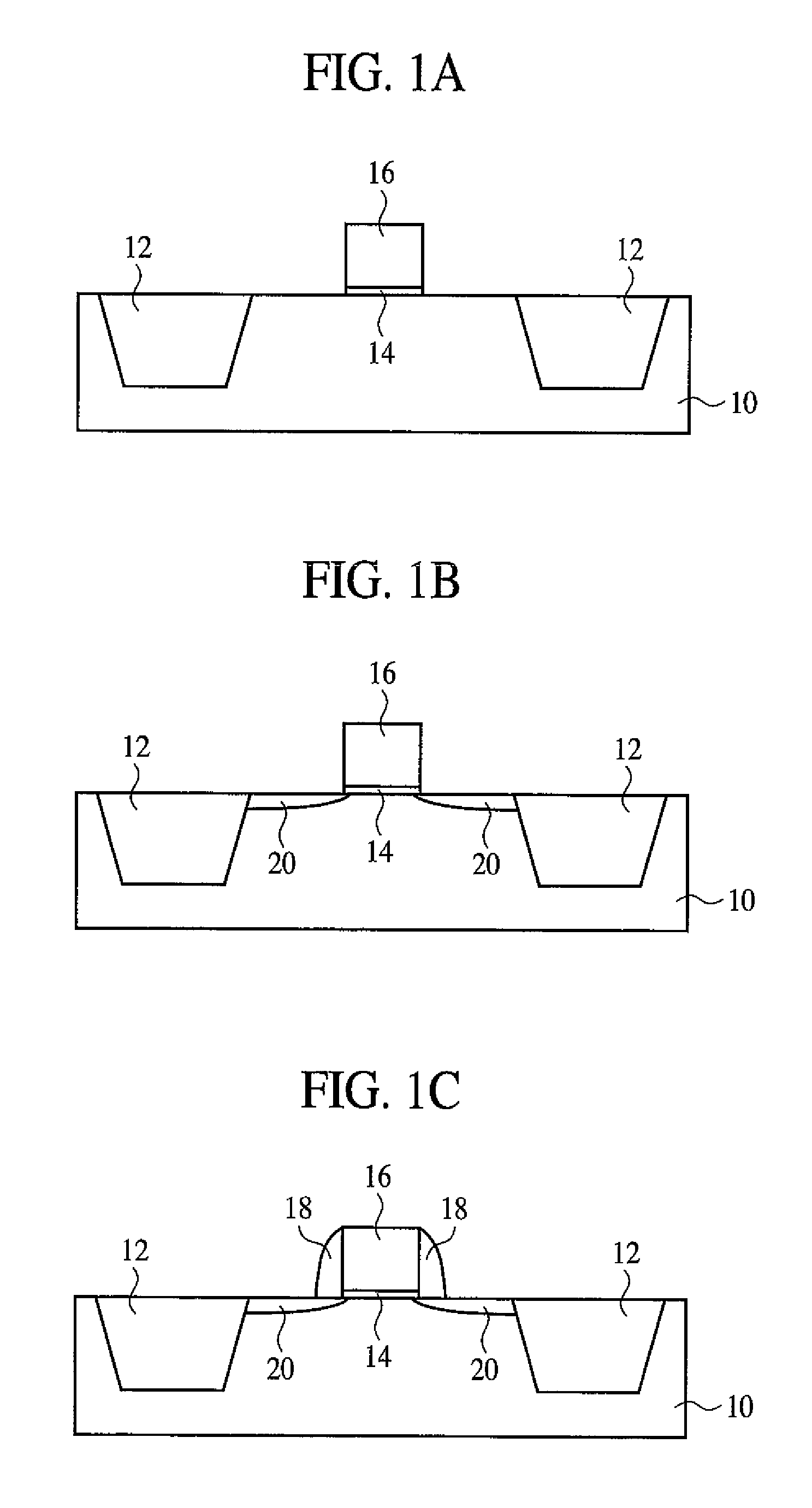
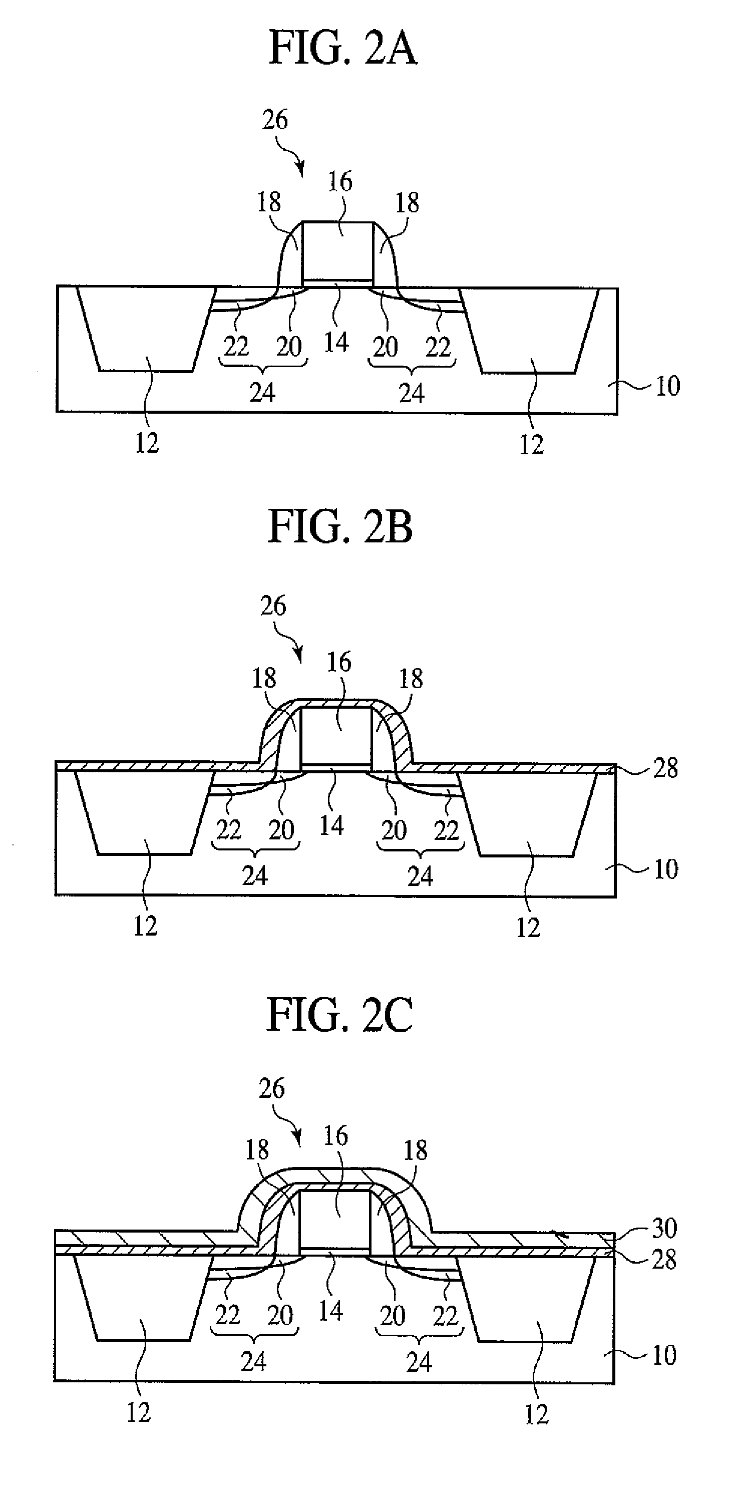
[0192]The method of manufacturing the semiconductor device according to a second embodiment of the present invention will be explained with reference to FIGS. 15A to 18B. FIGS. 15A-15C, 16A-16C, 17A-17C and 18A-18B are sectional views showing the steps of the method of manufacturing the semiconductor device according to the present embodiment. The same members of the present embodiment as those of the method of manufacturing the semiconductor device according to the first embodiment are represented by the same reference numbers not to repeat or to simplify their explanation.

[0193]The method of manufacturing the semiconductor device according to the present embodiment is characterized mainly in that compressive strain is introduced into the channel region of a PMOS transistor.

[0194]First, in the same way as in the method of manufacturing the semiconductor device according to the first embodiment shown in FIGS. 1A and 1B, in an NMOS transistor-to-be-formed region 60...

third embodiment

A Third Embodiment

[0241]The method of manufacturing the semiconductor device according to a third embodiment of the present invention will be explained with reference to FIGS. 20A to 22B. FIGS. 20A-20C, 21A-21C and 22A-22B are sectional views showing the steps of the method of manufacturing the semiconductor device according to the present embodiment. The same members of the present embodiment as those of the method of manufacturing the semiconductor device according to the first and the second embodiments are represented by the same reference numbers not to repeat or to simplify their explanation.

[0242]The method of manufacturing the semiconductor device according to the present embodiment is characterized mainly in that tensile strain is introduced into the channel region of an NMOS transistor.

[0243]In the same way as in the method of manufacturing the semiconductor device according to the second embodiment shown in FIG. 15A to FIG. 16A, in an NMOS transistor-to-be-formed region 6...


PUM

PropertyMeasurementUnit
concentrationaaaaaaaaaa

Abstract

The method of manufacturing the semiconductor device comprises forming a transistor including a gate electrode and a source / drain diffused layer over a semiconductor substrate, forming a nickel platinum film over the semiconductor substrate, covering the gate electrode and the source / drain diffused layer, making a first thermal processing to react the nickel platinum film with the source / drain diffused layer to form a nickel platinum silicide film, and removing an unreacted part of the nickel platinum film using a chemical liquid of 71° C. or more containing hydrogen peroxide.

Description

CROSS REFERENCE TO RELATED APPLICATIONS[0001]This application is based upon and claims the benefit of priorities from the prior Japanese Patent Application No. 2006-277424, filed on Oct. 11, 2006 and the prior Japanese Patent Application No. 2007-065402, filed on Mar. 14, 2007, the entire contents of which are incorporated herein by reference.BACKGROUND OF THE INVENTION[0002]The present invention relates to a method of manufacturing a semiconductor device, more specifically, a method of manufacturing a semiconductor device in which silicidation is made, and a method of manufacturing a semiconductor device in which a contact plug is formed, connected to a metal silicide film.[0003]As art of making a gate electrode and source / drain diffused layers with low resistivity, the process of forming metal silicide films on the surfaces of them by self-alignment, the so-called salicide (Self-Aligned Silicide) process is known. As metal materials to be reacted with silicon in the salicide proce...

Claims


Application Information

Patent Timeline
Patent Type & Authority Patents(United States)
IPC IPC(8): H01L21/44
CPCH01L29/7833H01L29/66636H01L21/28556H01L29/665H01L21/76862H01L21/28518H01L21/823814H01L21/823807H01L29/7848H01L21/76864H01L29/6659H01L21/823835H01L29/66545H01L21/32134H01L29/6656H01L21/76843
Inventor AKIYAMA, SHINICHIKAWAMURA, KAZUOUCHIDA, MASANORI
Owner FUJITSU SEMICON LTD
Learn More