Semiconductor device

a semiconductor device and semiconductor technology, applied in the direction of semiconductor devices, electrical devices, transistors, etc., can solve the problems of inability to maintain regular gate shape, increase in the layout area of the semiconductor device, uneven gate length, etc., to achieve reliably suppress uneven gate length and increase the layout area

Active Publication Date: 2014-04-08
SOCIONEXT INC
View PDF20 Cites 9 Cited by
  • Summary
  • Abstract
  • Description
  • Claims
  • Application Information

AI Technical Summary

Benefits of technology

[0016]According to the present invention, even when a well potential supply area is disposed, since it is possible to maintain regularity in the shapes of the peripheral gate patterns thereof, an increase in the layout area resulting from providing the well potential supply area can be suppressed while reliably suppressing unevenness in the gate length.

Problems solved by technology

For this reason, there occurs a problem in that the influence of the optical proximity effect significantly differs depending on the state of peripheral gate patterns, and unevenness in the gate length occurs.
However, when well potential supply cells are disposed in the related art, it is not possible to maintain regularity in the shapes of the gate patterns arranged in the lateral and longitudinal directions of the target gate.
In this case, however, an increase in the layout area of the semiconductor device is induced, which is not favorable.

Method used


Image

  • Semiconductor device
  • Semiconductor device
  • Semiconductor device

Examples


first exemplary embodiment

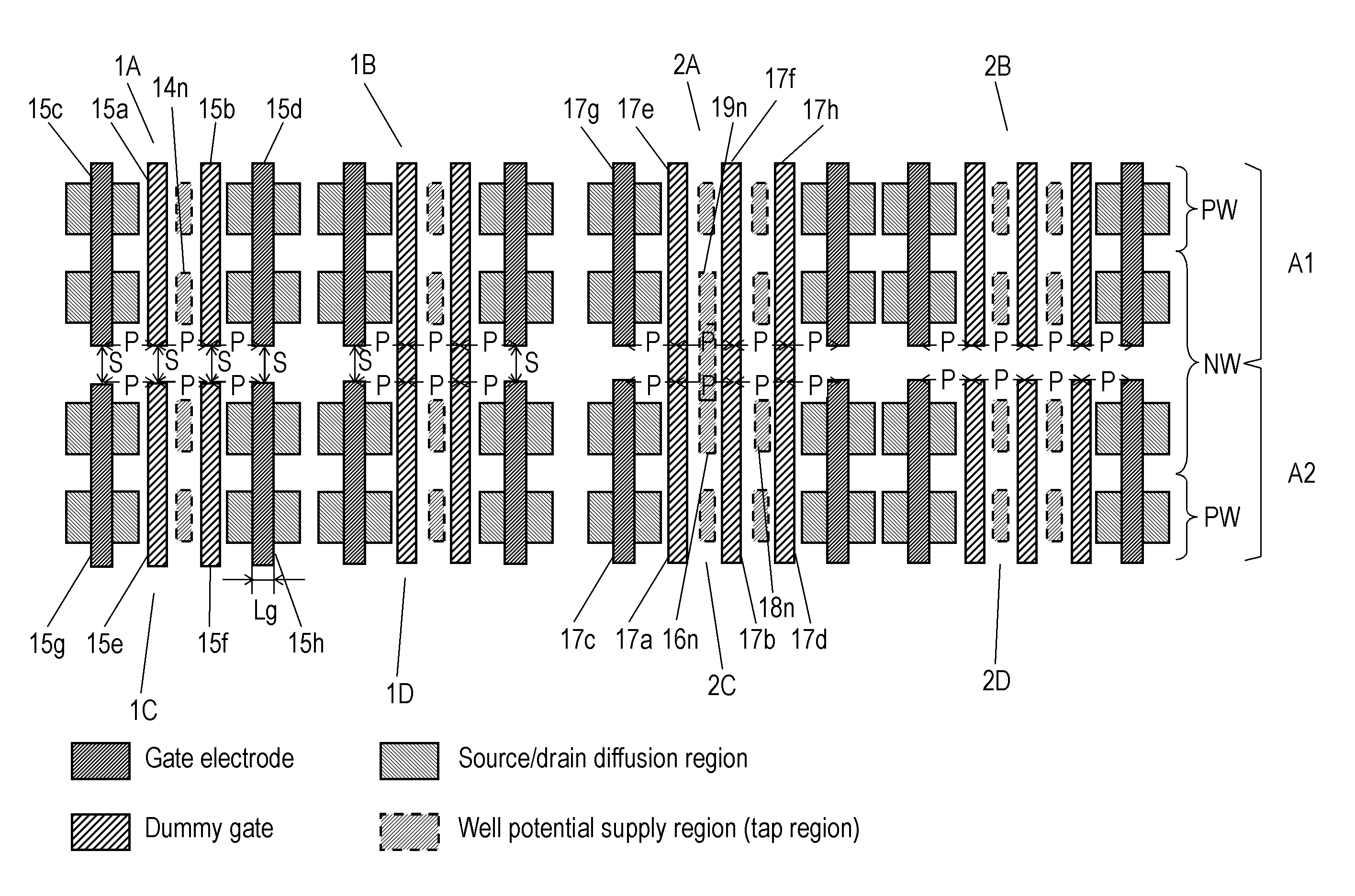
[0034]FIG. 1 is a drawing showing an example of the layout structure of a tap cell according to a first exemplary embodiment. Herein, a “tap cell” refers to a cell having a potential supply region to a well. In the layout structure of FIG. 1, tap cell 1 is closely disposed between logic cells 5a and 5b constituting an inverter.

[0035]In FIG. 1, tap cell 1 includes N-type impurity diffusion region 11n formed in N-type well region NW and P-type impurity diffusion region 11p formed in P-type well region PW. Desired well potential is supplied from N-type impurity diffusion region 11n to N-type well region NW via contacts and wiring. Desired well potential is supplied from P-type impurity diffusion region 11p to P-type well region PW via the contacts and wiring. In other words, N-type impurity diffusion region 11n and P-type impurity diffusion region 11p constitute a well potential supply region (TAP region).

[0036]Logic cells 5a and 5b respectively include PMOS transistors TPa and TPb for...

second exemplary embodiment

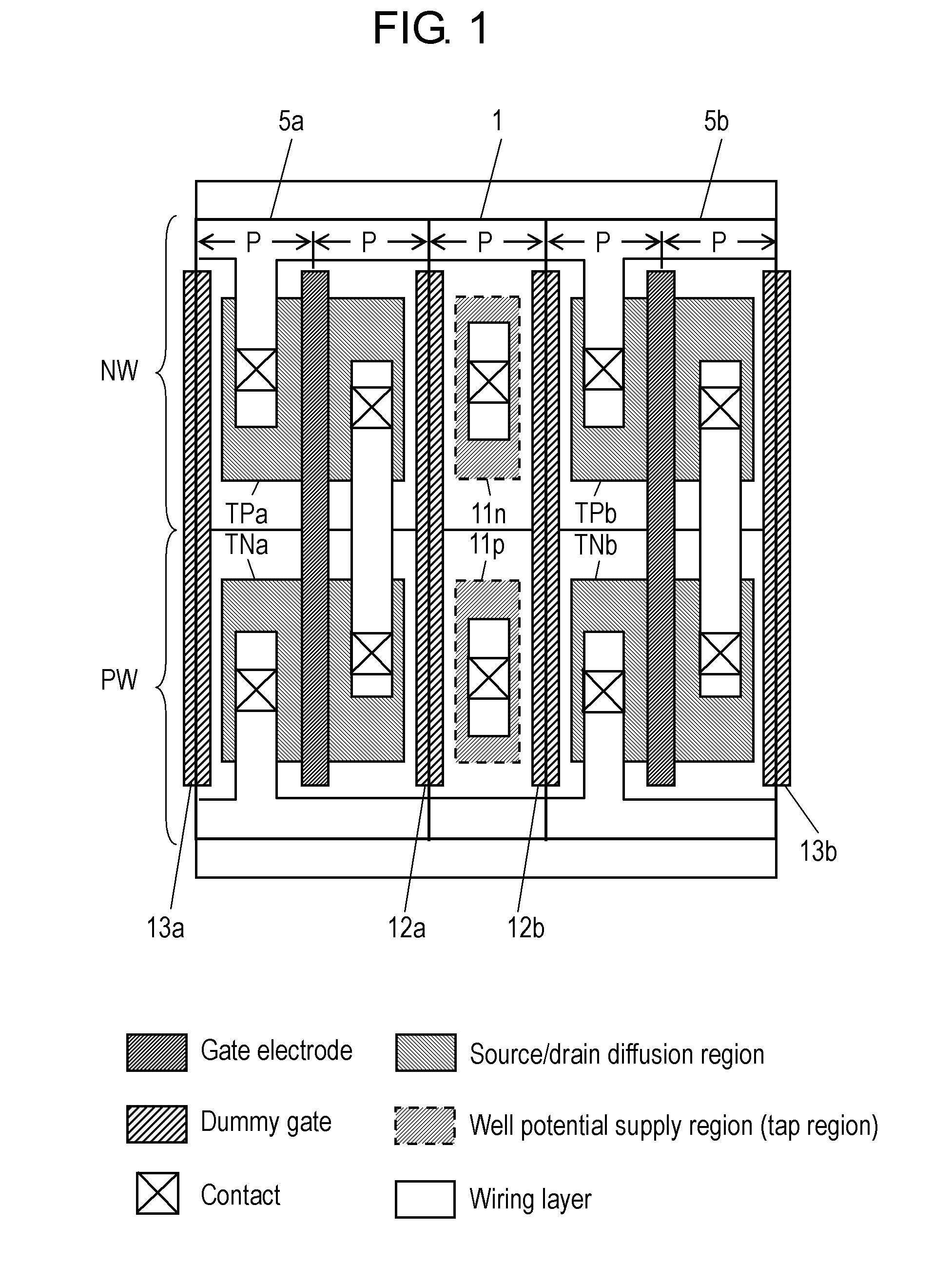
[0060]FIG. 6 is a diagram showing an example of the layout structure of a tap cell according to a second exemplary embodiment. In the layout structure of FIG. 6, tap cell 3 is closely disposed between logic cells 5a and 5b constituting an inverter. The layout structure of logic cells 5a and 5b is the same as in FIG. 1.

[0061]In FIG. 6, tap cell 3 includes N-type impurity diffusion region 31n formed in N-type well region NW and P-type impurity diffusion region 31p formed in P-type well region PW. Desired well potential is supplied from N-type impurity diffusion region 31n to N-type well region NW via contacts and wiring. Desired well potential is supplied from P-type impurity diffusion region 31p to P-type well region PW via the contacts and wiring. In other words, N-type impurity diffusion region 31n and P-type impurity diffusion region 31p constitute a well potential supply region (TAP region).

[0062]In addition, dummy gates 32a and 32b are respectively disposed between tap cell 3 an...

example 1

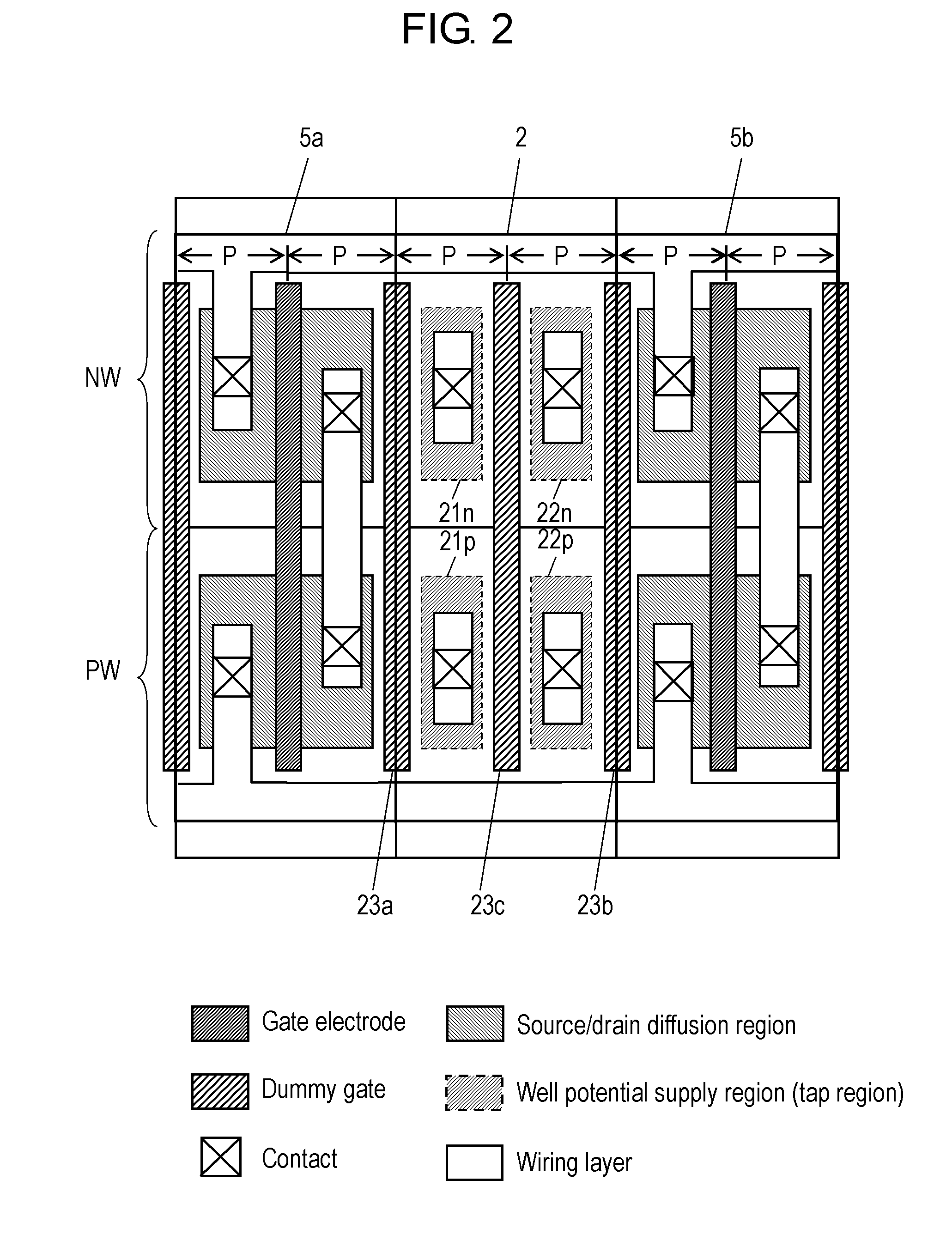
[0068]FIG. 8 is another example of the layout structure of the semiconductor device. In the layout of FIG. 8, cell arrays C1, C2, and C3, in which a plurality of gates extending in the vertical direction are arranged and disposed in the horizontal direction, are arranged and disposed in the vertical direction in the same manner as in FIG. 7. In cell arrays C1, C2, and C3, P-type well regions PW and N-type well regions NW extending in the horizontal direction are respectively formed below the gates. Furthermore, in cell array C2, P-type well region PW and N-type well region NW are flipped so as to make N-type well regions NW of cell arrays C1 and C2 adjacent to each other and make P-type well regions PW of cell arrays C2 and C3 adjacent to each other.

[0069]One of the characteristics of the layout structure of FIG. 8 is P-type impurity diffusion region 41p and N-type impurity diffusion region 41n. P-type impurity diffusion region 41p performs power-supply to P-type well region PW of c...


PUM


Abstract

A well potential supply region is provided in an N-type well region of a cell array. Adjacent gates disposed in both sides of the well potential supply region in the horizontal direction and adjacent gates disposed in further both sides thereof are disposed at the same pitch. In addition, an adjacent cell array includes four gates each of which is opposed to the adjacent gates in the vertical direction. In other words, regularity in the shape of the gate patterns in the periphery of the well potential supply region is maintained.

Description

BACKGROUND[0001]1. Technical Field[0002]The present invention relates to a semiconductor device provided with a well potential supply region for supplying power to a well region.[0003]2. Background Art[0004]In a semiconductor device of the related art, there is provided a well potential supply region for supplying power to a well region in the vicinity of an active transistor for the purpose of controlling well potential, in other words, for the purpose of preventing latch-up. Furthermore, the “active transistor” refers to a transistor that contributes to a desired function of a circuit using the operation characteristic of the transistor.[0005]FIG. 12 is a diagram showing an example of a layout of a semiconductor device of the related art, in which a well potential supply region is provided. In the configuration of FIG. 12, standard cell arrays in which a plurality of standard cells are disposed in the horizontal direction of the drawing are disposed by being arranged in the vertic...

Claims


Application Information

Patent Timeline
Patent Type & Authority Patents(United States)
IPC IPC(8): H01L27/088
CPCH01L27/0207H01L27/11898H01L21/823892H01L27/11807H01L27/0928H01L2027/11866H01L2027/11881H01L2027/1189
Inventor TAMARU, MASAKINAKANISHI, KAZUYUKINISHIMURA, HIDETOSHI
Owner SOCIONEXT INC
Why Eureka
Try Eureka