Bulk acoustic wave resonator and method of fabricating same
a resonator and acoustic wave technology, applied in the direction of generator/motor, piezoelectric/electrostrictive transducer, transducer type, etc., can solve the problem of reducing the robustness of esd of the resonator, the pz layer cracks significantly reducing the esd robustness, and the tensile strength of the resonator is serious
- Summary
- Abstract
- Description
- Claims
- Application Information
AI Technical Summary
Benefits of technology
Problems solved by technology
Method used
Image
Examples
first embodiment
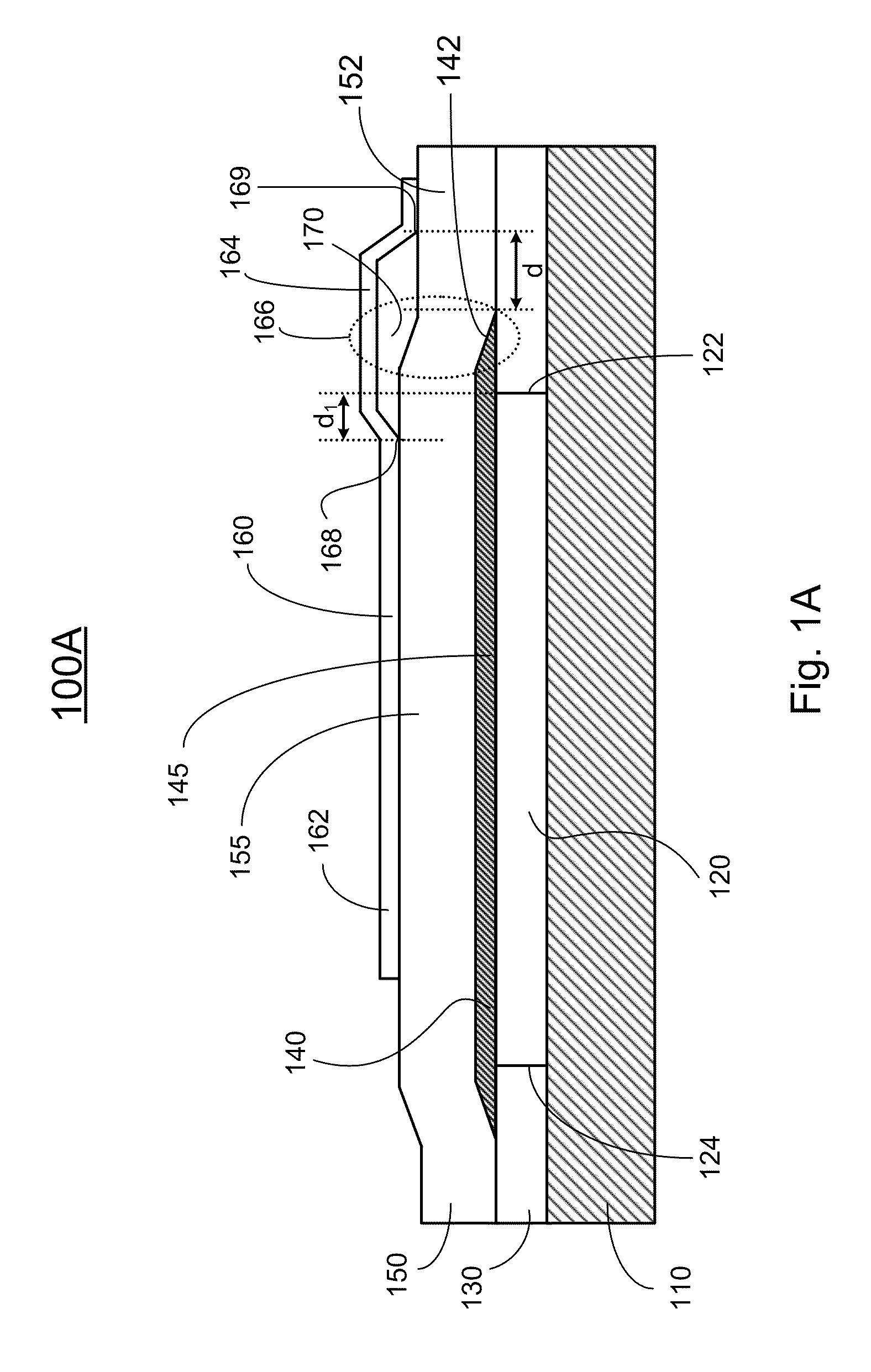
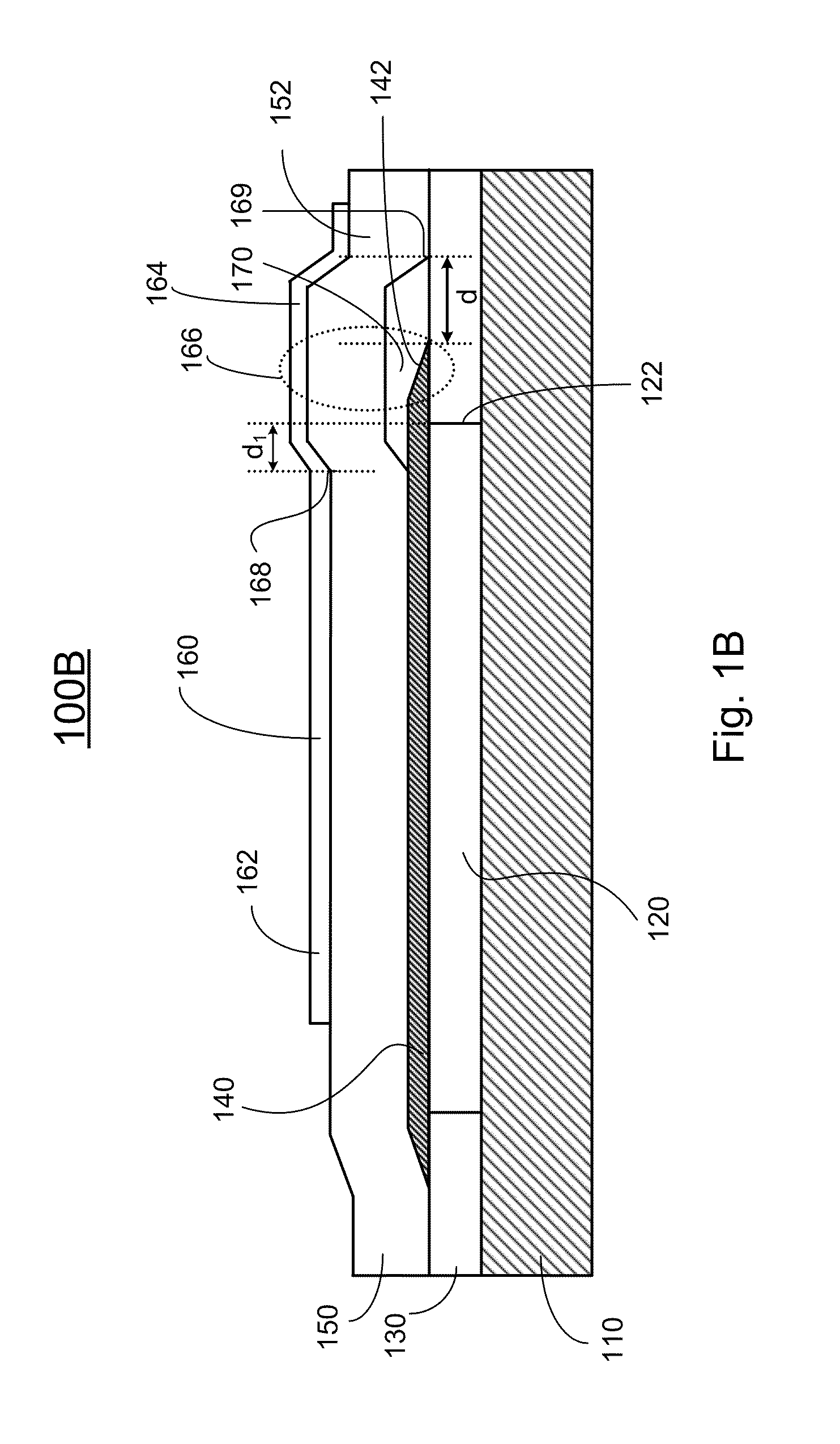
[0054]Referring now to FIG. 1A, a BAW resonator 100A is shown according to the present invention. The BAW resonator 100 includes a substrate 110 and an acoustic mirror 120 that is formed on a top surface of the substrate 110 or in the substrate 110. Although the acoustic mirror 120 as shown in FIG. 1A is provided by an air cavity 120 defined between the substrate 110 and the dielectric layer 130 deposited on the top surface of the substrate 110, it would be appreciated that any other acoustic mirror structure such as a Bragg reflector is also applicable.
[0055]The BAW resonator 100A also includes a first electrode 140, a piezoelectric layer 150 and a second electrode 160. The first electrode 140 is deposited on the top surface of the dielectric layer 130 and overlapping the acoustic mirror 120. The first electrode 140 may be etched to form a tapered end portion 142, which extends beyond the contour / edge 122 of the acoustic mirror 120. Additionally, the first electrode 140 may be form...
second embodiment
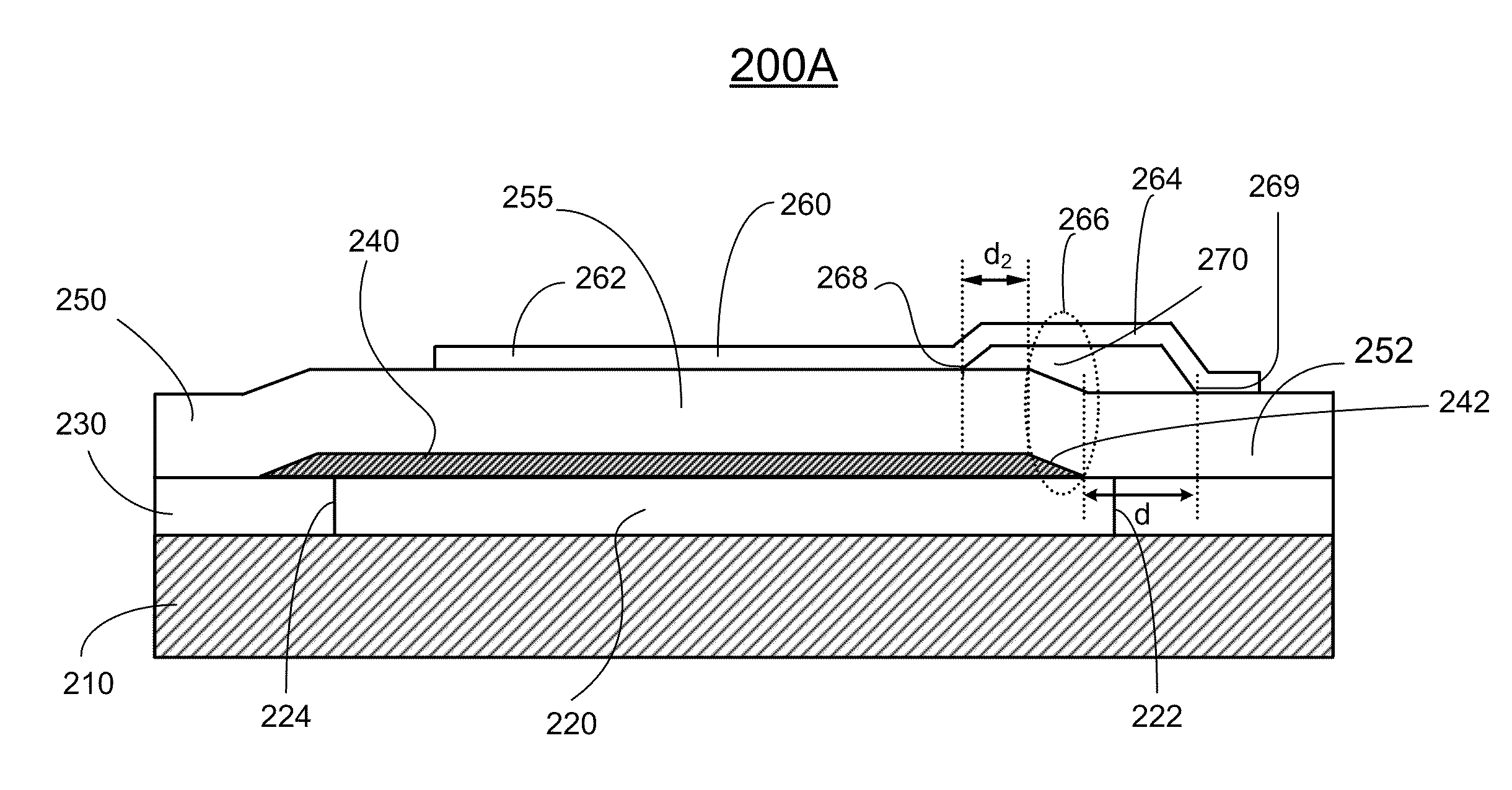
[0059]Referring to FIG. 2A, a BAW resonator 200A is shown according to the present invention. The BAW resonator 200A comprises a substrate 210, an acoustic mirror 220 formed in or on the substrate 210, having a first edge 222 and an opposite, second edge 224, a dielectric layer 230 formed on the substrate 210 such that the dielectric layer 230 is substantially in contact with the first and second edges of the acoustic mirror 220, a first electrode 240 formed on the acoustic mirror 220, having a first end portion 242 and an opposite, second end portion defining a body portion therebetween, where the first end portion 242 is located between the first edge 222 and the second edge 224 of the acoustic mirror 220, a piezoelectric layer 250 formed on the first electrode 240, having a body portion 255, a first end portion 252 and a second end portion oppositely extending from the body portion onto the dielectric layer 230; and a second electrode 260 formed on the piezoelectric layer 250, ha...
fourth embodiment
[0067]Referring now to FIG. 4, a BAW resonator 400 is shown according to the present invention. The BAW resonator 400 comprises a substrate 410 having an acoustic mirror 420 in or on a top surface thereof. While the acoustic mirror 420 as shown in FIG. 4 is provided by an air cavity 420 in the dielectric layer 430 deposited on the top surface of the substrate 410, any other acoustic mirror structure such as a Bragg reflector is also applicable. A first electrode 440 is deposited on the dielectric layer 430 and over the acoustic mirror 420, and the first electrode 440 is etched forming a tapered end portion 442. Additionally, an tapered end portion edge 448 of the first electrode 440 terminates within the contour 422 of the acoustic mirror 420, i.e., there is a distance (d3) between the tapered end portion edge 448 of the first electrode and the corresponding contour 422 of the acoustic mirror 420.
[0068]A piezoelectric layer 450 is deposited on the first electrode 440. The piezoelect...
PUM
| Property | Measurement | Unit |
|---|---|---|
| piezoelectric | aaaaa | aaaaa |
| thicknesses | aaaaa | aaaaa |
| distance | aaaaa | aaaaa |
Abstract
Description
Claims
Application Information


