Supercharge Your Innovation With Domain-Expert AI Agents!

Implant for performance enhancement of selected transistors in an integrated circuit

a technology of integrated circuits and transistors, applied in the field of integrated circuits, can solve problems such as incomplete accuracy and inability to perform precisely in integrated circuits

Inactive Publication Date: 2014-04-29
NXP USA INC
View PDF12 Cites 0 Cited by
  • Summary
  • Abstract
  • Description
  • Claims
  • Application Information

AI Technical Summary

Benefits of technology

The patent text describes a technique for improving the performance of selected transistors in an integrated circuit without replacing all or some portion of the mask set. The technique involves using an implant to change the characteristics of the transistors to more desirable levels. By doing so, the integrated circuit can achieve better performance without the need for a complete overhaul of the mask set. The semiconductor device described in the patent text includes a semiconductor substrate with transistors formed therein. The transistors have different channel widths, which affects their performance. The technique allows for the adjustment of the transistor characteristics to improve performance without changing the overall leakage of the transistors. The semiconductor device can be made with various semiconductor materials or combinations of materials.

Problems solved by technology

Sometimes the models are not completely accurate so that the integrated circuit may not perform precisely as predicted or further performance changes may be found to be desirable after having been field tested.
This may result in the need for replacing one or more of the masks in the mask set to correct the identified issue because at least some portion of the initial mask set will be unusable.

Method used


Image

  • Implant for performance enhancement of selected transistors in an integrated circuit
  • Implant for performance enhancement of selected transistors in an integrated circuit
  • Implant for performance enhancement of selected transistors in an integrated circuit

Examples


Embodiment Construction

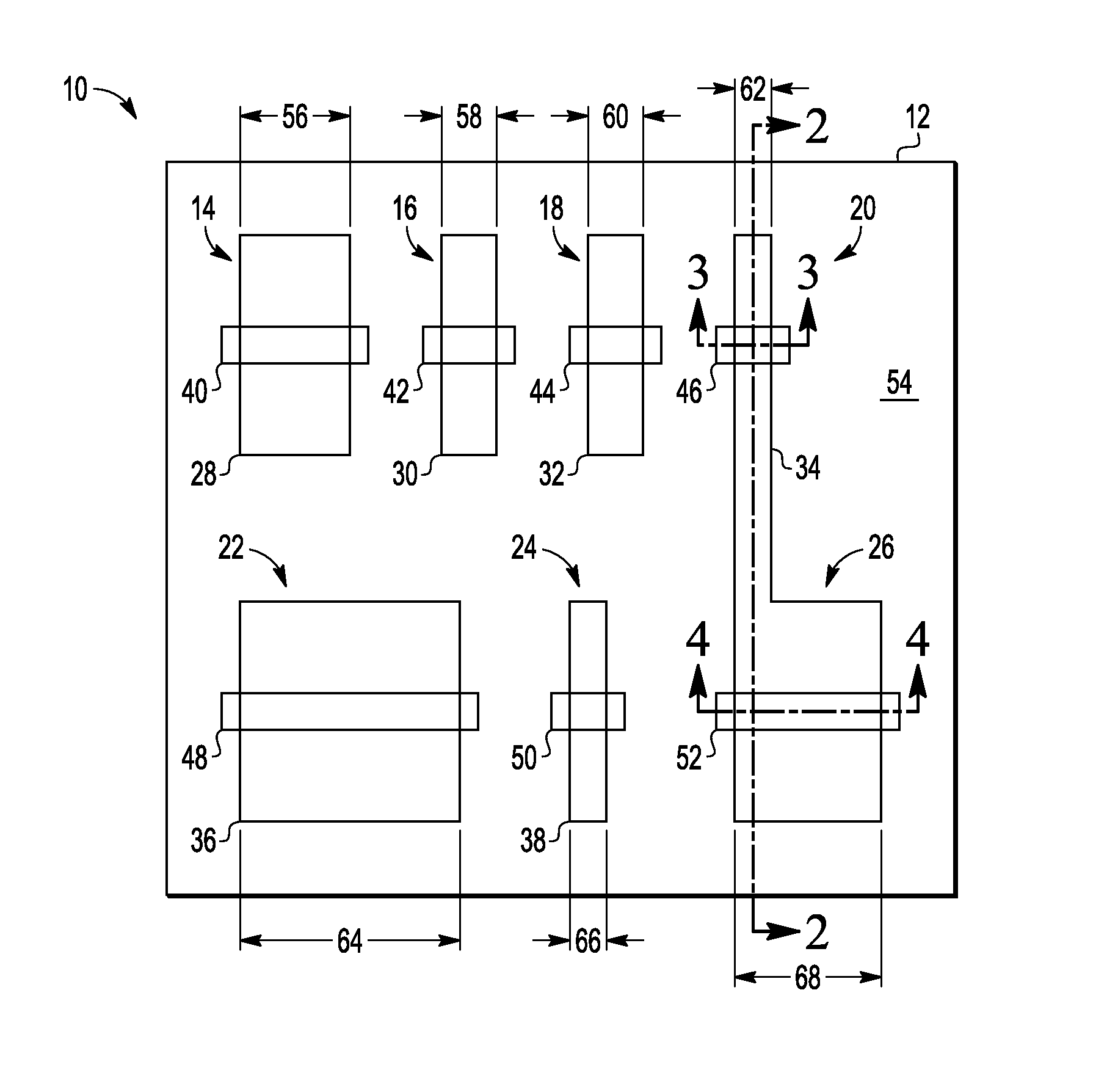
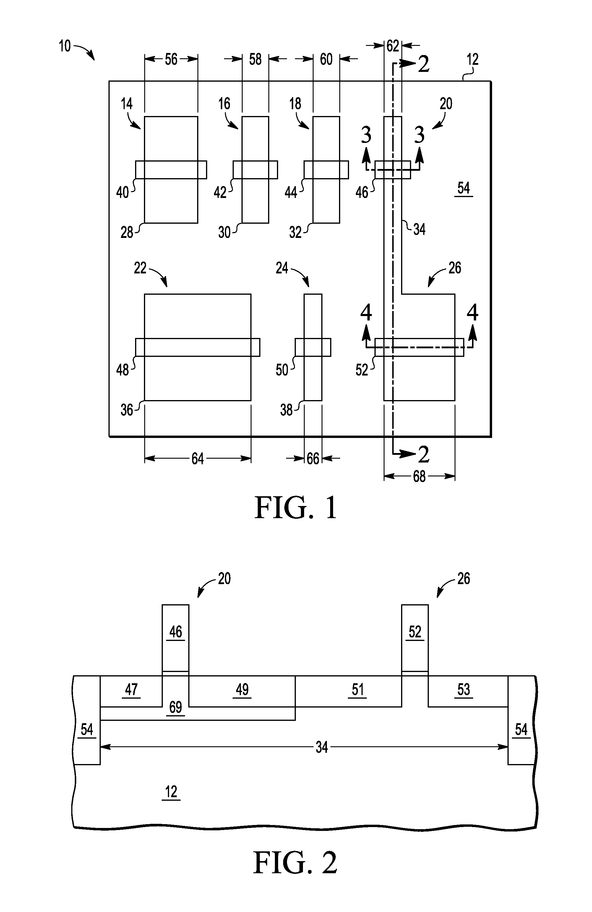
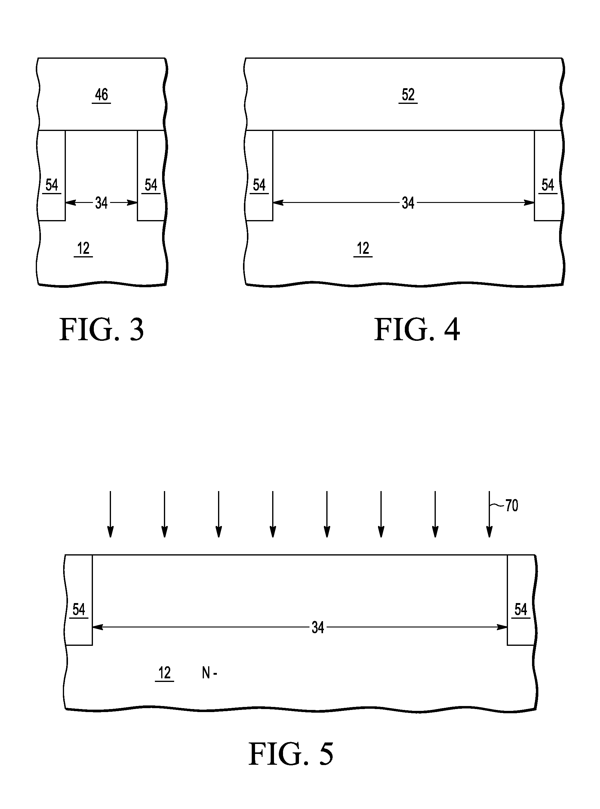
[0014]A semiconductor device has a plurality of transistors of a first conductivity type in a well that has a background doping. Transistors within that well that have a channel width less than predetermined dimension are doped to reduce the threshold voltage and increase the drive current of those transistors. Although this may have the effect of increasing leakage of those implanted transistors, the overall leakage is only increased by a small amount because these are the smallest transistors and the number of transistors receiving this implant can be a relatively small number of the total number of transistors. This can be used to improve the performance of an existing design that may already be in production. This is better understood by reference to the drawings and the following description.

[0015]The semiconductor substrate described herein can be any semiconductor material or combinations of materials, such as gallium arsenide, silicon germanium, silicon-on-insulator (SOI), s...


PUM


Abstract

A first implant is performed into a substrate to form a well in which a plurality of transistors will be formed. Each transistor of a first subset of the plurality of transistors to be formed has a width that satisfies a predetermined width constraint and each transistor of a second subset has a width that does not satisfy the constraint. A second implant is performed at locations in the well in which transistors of the first subset will be formed and not at locations in the well in which transistors of the second subset will be formed. The transistors are formed, wherein a channel region of each transistor of the first subset is formed in a portion of the substrate which received the second implant and a channel region of each transistor of the second subset is formed in a portion of the substrate which did not receive the second implant.

Description

BACKGROUND[0001]1. Field[0002]This disclosure relates generally to integrated circuits, and more specifically, to enhanced performance of selected transistors of the integrated circuit by use of an implant.[0003]2. Related Art[0004]Integrated circuits are designed with an expectation of transistor characteristics based on experiments with regard to the anticipated process and modeling of the transistor performance. Sometimes the models are not completely accurate so that the integrated circuit may not perform precisely as predicted or further performance changes may be found to be desirable after having been field tested. This may result in the need for replacing one or more of the masks in the mask set to correct the identified issue because at least some portion of the initial mask set will be unusable.[0005]Accordingly, there is a need to provide a technique that allows for changing transistor characteristics to more desired characteristics without requiring replacement of all or...

Claims


Application Information

Patent Timeline
Patent Type & Authority Patents(United States)
IPC IPC(8): H01L21/00H01L21/84
CPCH01L21/823412H01L21/823493H01L27/0207H01L27/088
Inventor SHROFF, MEHUL D.JOHNSTONE, WILLIAM F.WEINTRAUB, CHAD E.
Owner NXP USA INC
Features
  • R&D
  • Intellectual Property
  • Life Sciences
  • Materials
  • Tech Scout
  • Unparalleled Data Quality
  • Higher Quality Content
  • 60% Fewer Hallucinations
Learn More