
Area efficient power switch

a power switch and area-efficient technology, applied in the field of integrated circuit layout and design, can solve the problems of limiting the amount of component size reduction or component modification to increase functionality without increasing the size of components

Inactive Publication Date: 2014-05-13
APPLE INC
View PDF7 Cites 9 Cited by
  • Summary
  • Abstract
  • Description
  • Claims
  • Application Information

AI Technical Summary

Benefits of technology

The present patent provides methods for generating an area efficient power switch cell for a cell library and an integrated circuit layout that utilizes the power switch cell. The power switch cell is designed by receiving a specification of a power switch circuit, with attributes such as a height of the cell boundary. The cell library design tool generates the power switch cell based on the specification and layout placement constraints. The integrated circuit layout then places the power switch cell and standard cells based on the placement constraints and doping type. The power switch cell and standard cell are placed adjacent to each other, with the standard cell facing the power switch cell and the substrate in a complementary manner. The technical effects of this patent include reducing the area of power switch cells in a cell library and optimizing the placement of power switch cells and standard cells in an integrated circuit layout.

Problems solved by technology

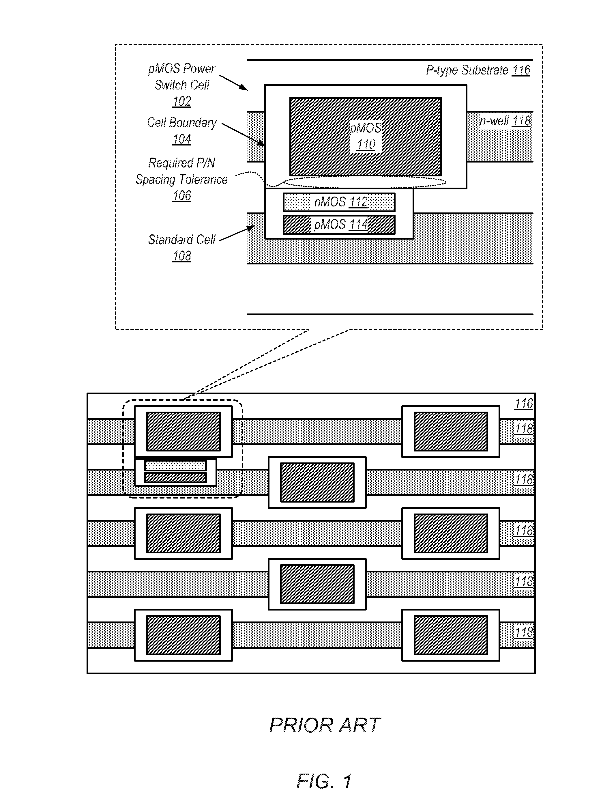
Integrated circuit layout designers, however, are often faced with challenges that limit the amount reduction in size of components or modifications to components to increase functionality without increasing the size of the components. FIG. 1, for example, sets forth a line drawing of a birds-eye view of a prior art integrated circuit layout.

Method used


Image

  • Area efficient power switch
  • Area efficient power switch
  • Area efficient power switch

Examples


Embodiment Construction

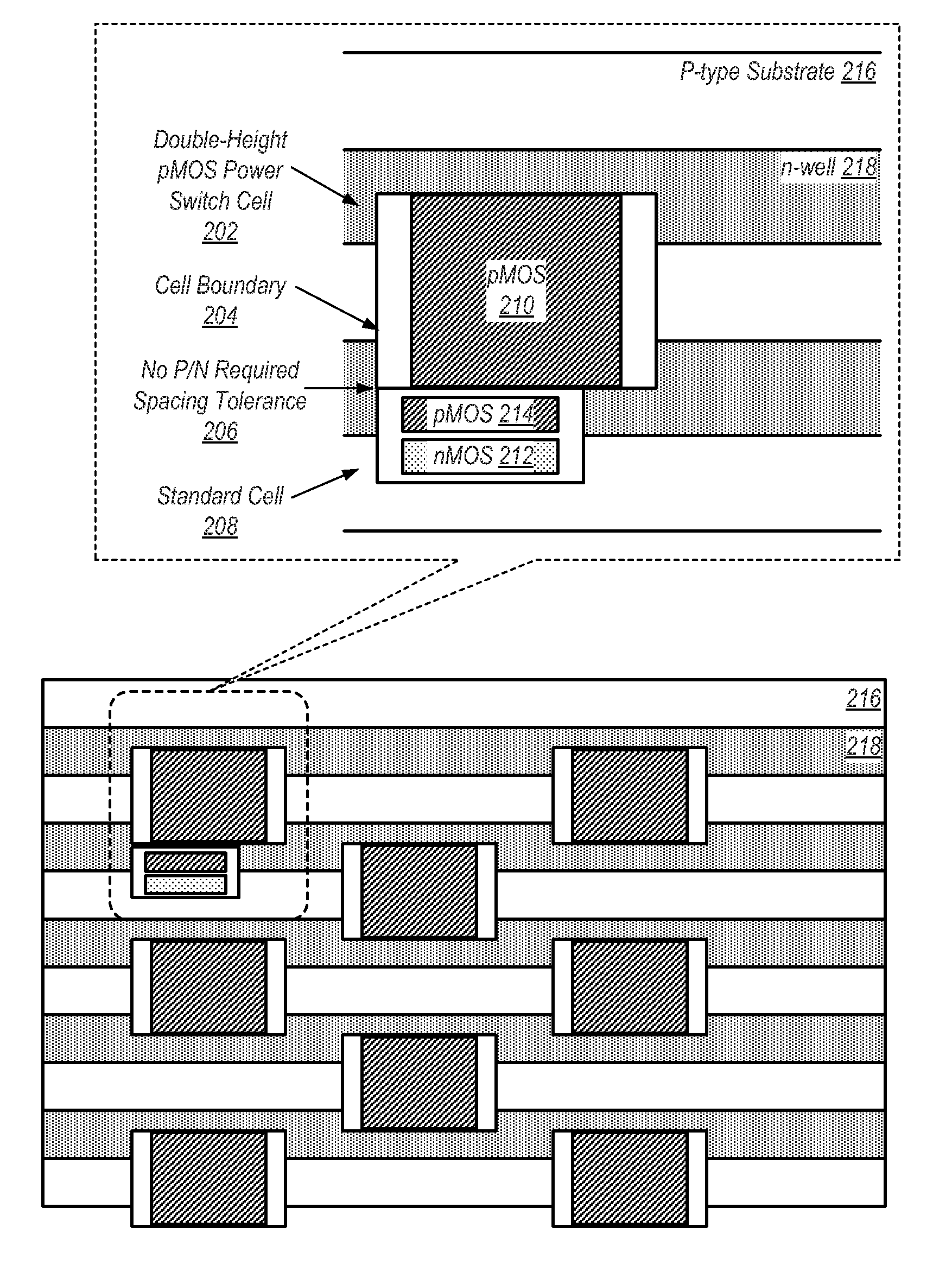
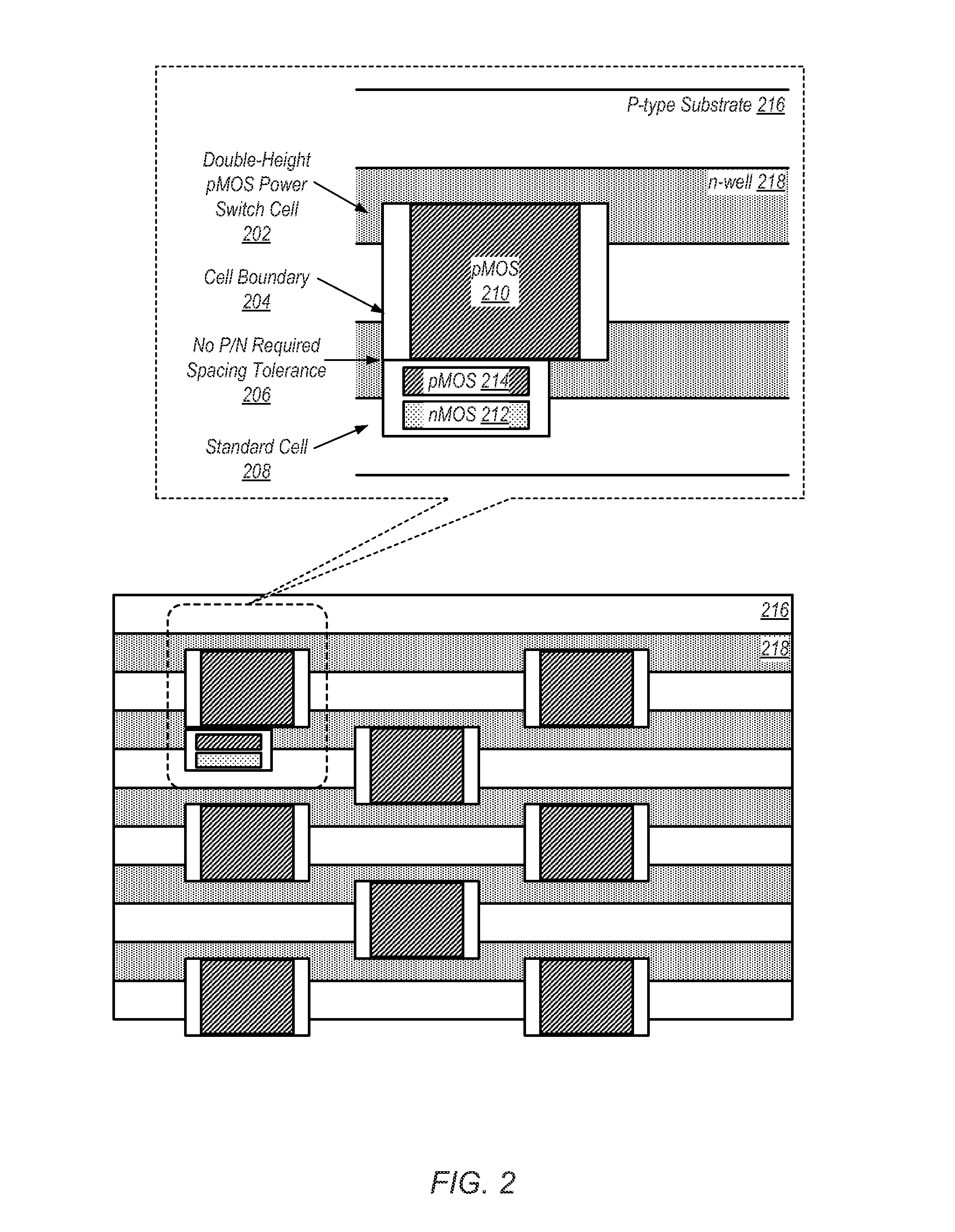
[0028]FIG. 2 sets forth a line drawing of an example integrated circuit layout with a double-height area efficient power switch. The example integrated circuit layout of FIG. 2 includes a number of pMOS-based power switch cells 202 and one standard cell 208. A ‘cell’ as the term is used here refers to representation of logic for use in integrated circuit design, simulation, and fabrication. A cell may represent logic in a variety of ways. A cell, for example, may represent logic's electrical schematic via a netlist, functionality, physical attributes, layout characteristics, operational timing characteristics, and the like. A ‘cell’ may be included in a library of cells for use by integrated circuit designers. A cell may be included in a library of cells for use by an integrated circuit designer. A cell may represent abstract more complicated circuits as a single functional block of logic. A standard cell for example may represent a single AND gate, OR gate, XOR gate, XNOR gate, inv...


PUM


Abstract

A method of generating an area efficient power switch cell includes receiving, by a cell library design tool, a specification of a power switch circuit to be established as a power switch cell in a cell library. The cell library design tool also receives one or more attributes of the power switch cell including a height of the cell boundary and receiving, by the cell library design tool, a layout placement constraint requiring the power switch cell to be placed in a semiconductor layout so as to bridge two parallel rows of doped wells. The parallel rows of doped wells are interleaved with doped substrate and the doping of the wells is of a different type than that of the substrate. Based on the specification of the power switch circuit, the one or more attributes, and the layout placement constraint, the cell library design tool generates the power switch cell.

Description

BACKGROUND[0001]1. Technical Field[0002]This disclosure relates generally to integrated circuit layouts and design, and more particularly to methods, systems, and products for generating an area efficient power switch cell of a cell library and for generating an integrated circuit layout for fabrication.[0003]2. Description of the Related Art[0004]In recent years, mobile devices such as smart phones and tablet computers have become increasingly sophisticated. In addition to supporting telephone calls, many mobile devices now provide access to the internet, email, text messaging, and navigation using the global positioning system (GPS). Mobile devices that support such sophisticated functionality often include many components. To remain a mobile, physical size of such components of a mobile device is a design concern. Designers of such mobile devices, often attempt to reduce the size of components or modify the components to provide greater functionality without increasing the size o...

Claims


Application Information

Patent Timeline
Patent Type & Authority Patents(United States)
IPC IPC(8): G06F17/50
CPCG06F17/5072G06F17/50G06F30/392
Inventor SUZUKI, SHINGORAJAGOPAL, KARTHIKTANG, BO
Owner APPLE INC
Learn More