Method and system for recycling processing gas for selenization of thin film photovoltaic materials

Inactive Publication Date: 2014-05-20
CM MFG
View PDF280 Cites 8 Cited by
  • Summary
  • Abstract
  • Description
  • Claims
  • Application Information

AI Technical Summary

Benefits of technology

[0007]It is to be appreciated that the present invention provides numerous benefits over conventional techniques. Among other things, the system and process of the present invention are compatible with conventional systems, which allow cost effective implementation. In various embodiments, the system

Problems solved by technology

In the process of manufacturing CIS and/or CIGS types of thin films, there are various manufacturing challenges, such as performing large scale thermal reactive treatment in a gaseous environment, maintaining structure integrity of substrate materials with extra large form factors, ensuring uniformity and granula

Method used


Image

  • Method and system for recycling processing gas for selenization of thin film photovoltaic materials
  • Method and system for recycling processing gas for selenization of thin film photovoltaic materials
  • Method and system for recycling processing gas for selenization of thin film photovoltaic materials

Examples


Embodiment Construction

[0010]The present invention relates generally to thin-film photovoltaic techniques. More particularly, the present invention provides a system and method for handling work gas used for the manufacture of thin-film photovoltaic devices based on copper indium diselenide species (CIS), copper indium gallium diselenide species (CIGS), and / or others. The invention can be applied to made CIGS photovoltaic modules on panels, flexible sheets, building or window glass, automotive, and others.

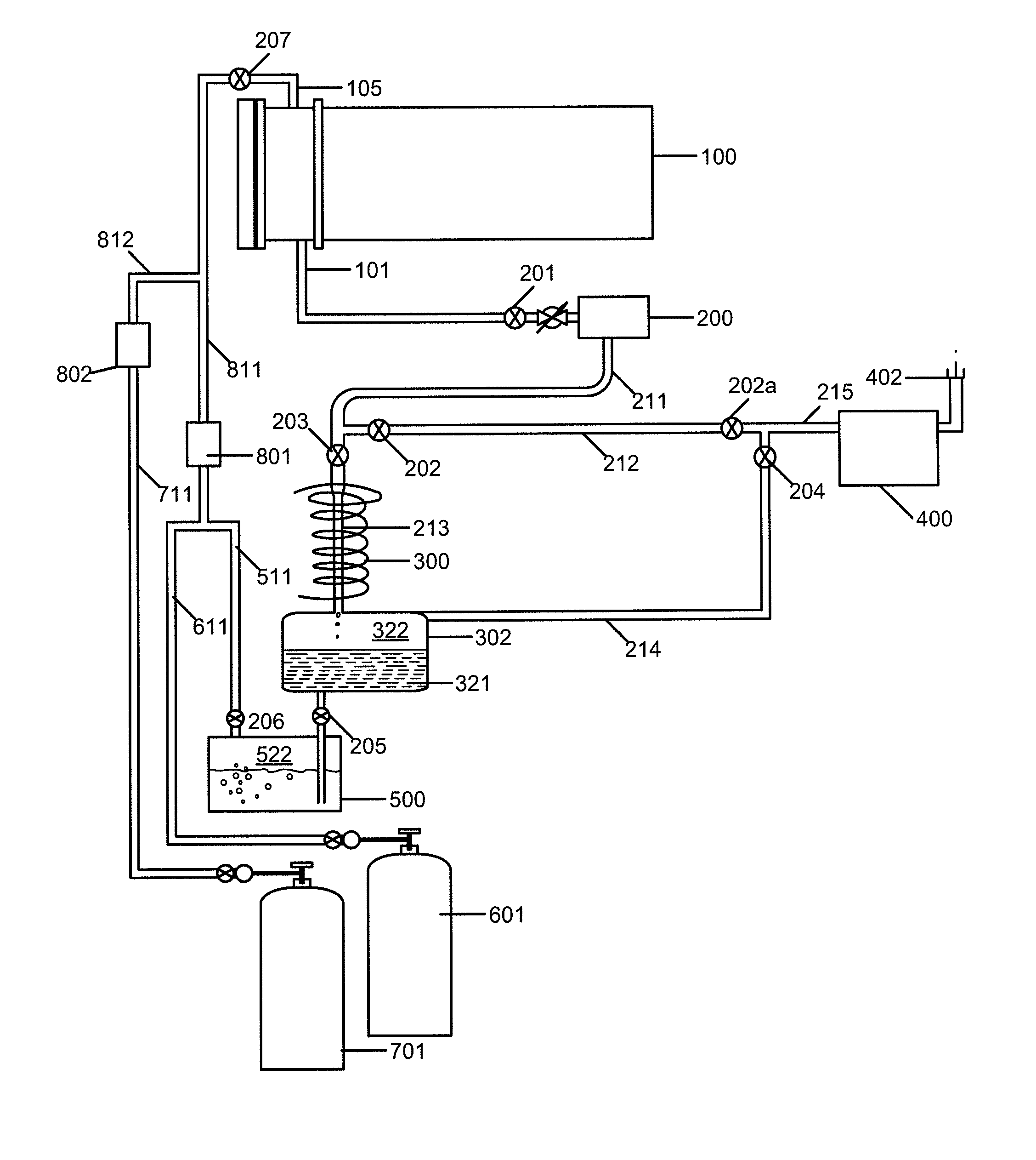
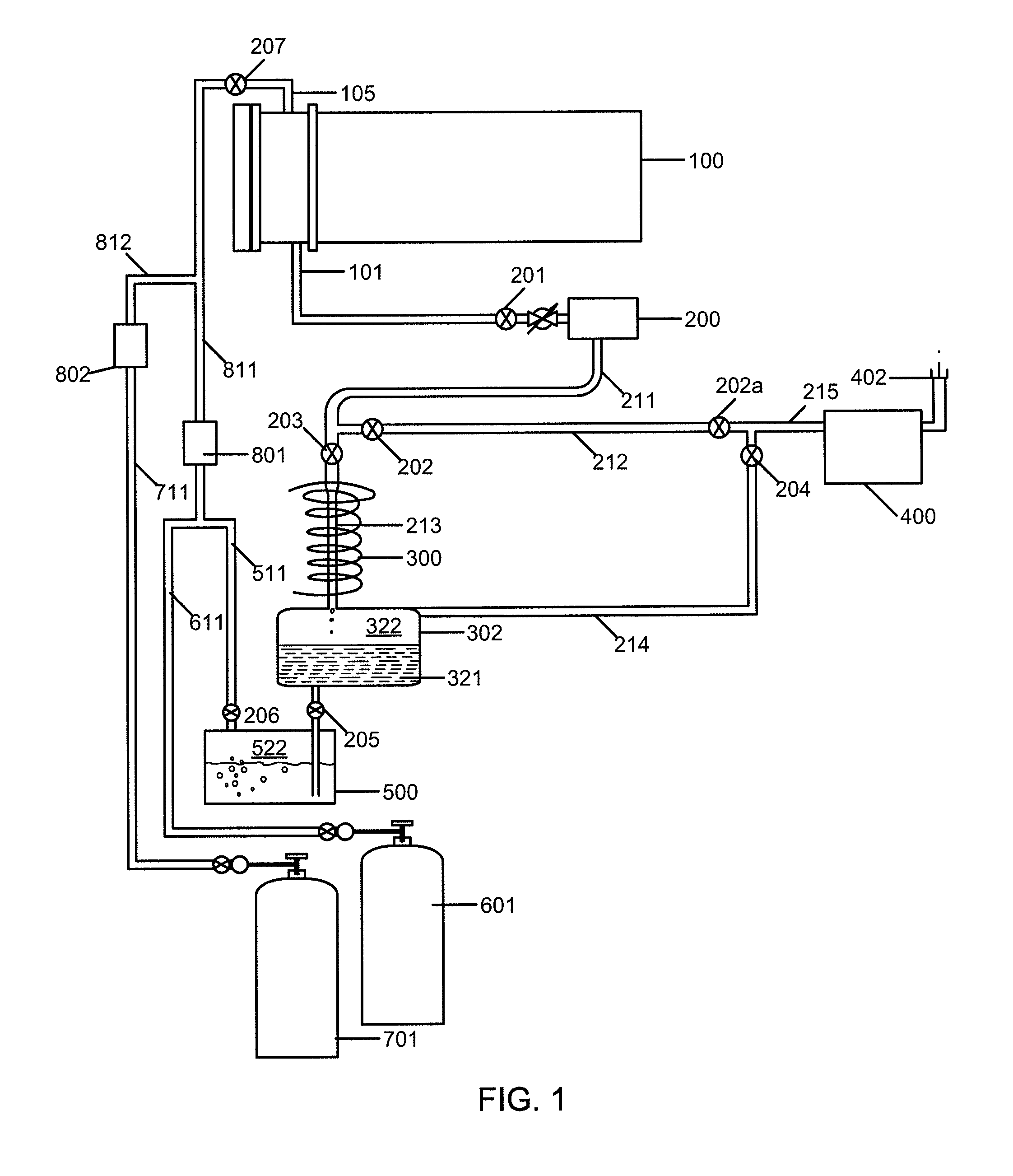
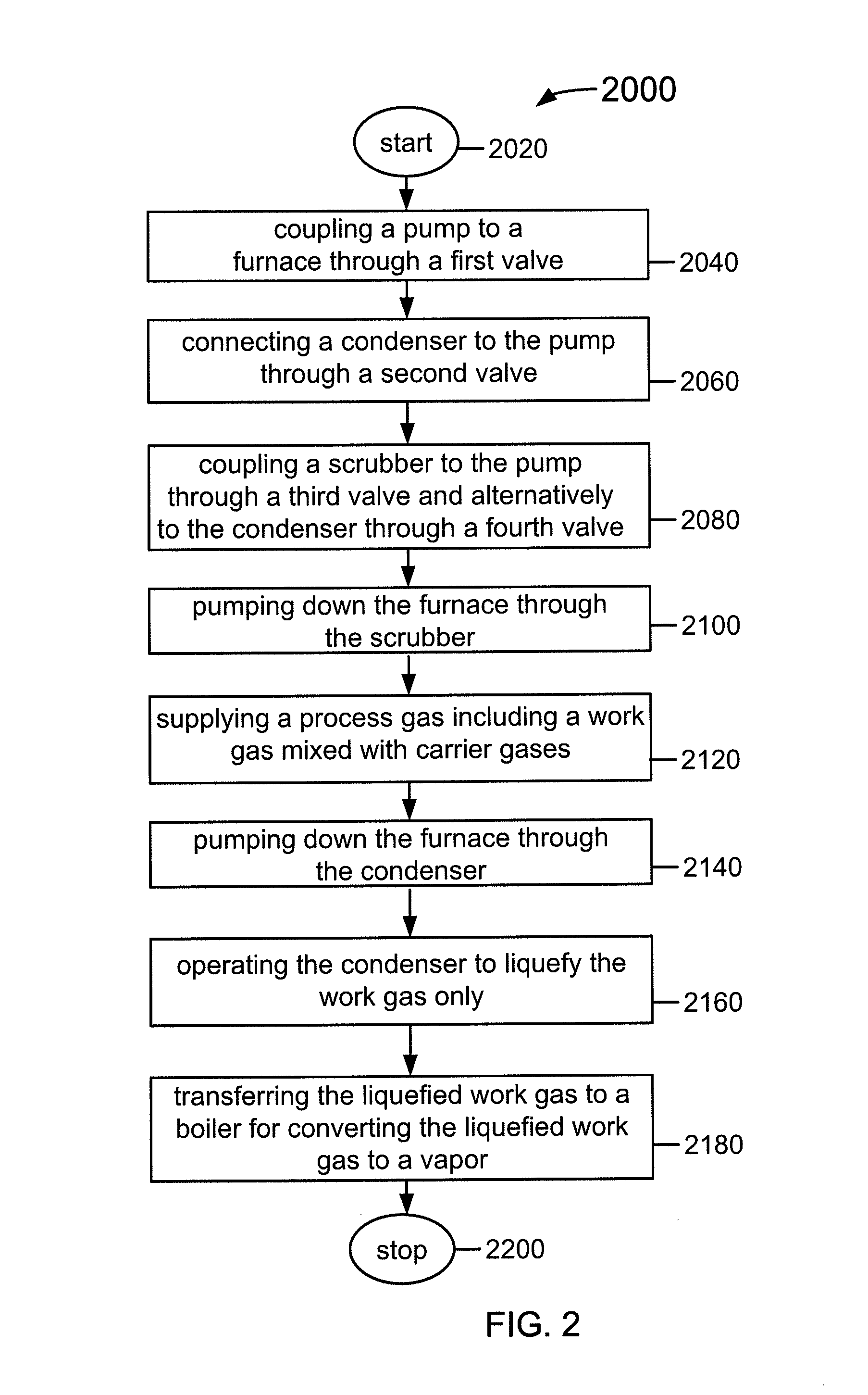
[0011]FIG. 1 is a diagram of a system for recycling a work gas for the manufacture of CIGS photovoltaic device according to an embodiment of the present invention. As shown, the system 1000 is associated with a process furnace or thermal reactor 100 that is configured to perform thermal reactive treatment of thin-film devices under a gaseous environment within the furnace. In an example, the thermal reactor 100 is applied to treat thin-film photovoltaic devices using a process gas 101 comprising a mixtur...


PUM

PropertyMeasurementUnit
Temperatureaaaaaaaaaa
Fractionaaaaaaaaaa
Pressureaaaaaaaaaa

Abstract

A system for recycling a work gas used in a thermal reactor for treating sample materials includes a thermal reactor using a work gas from a first source mixed with carrier gases. The work gas has a boiling point higher than the carrier gases. The system includes a pump, a condenser which converts the work gas into a liquid, and a scrubber.

Description

CROSS-REFERENCE TO RELATED APPLICATION[0001]This application claims priority to U.S. Provisional Patent Application No. 61 / 432,869, filed Jan. 14, 2011, commonly assigned, and hereby incorporated by reference in its entirety herein for all purpose.BACKGROUND OF THE INVENTION[0002]The present invention relates generally to thin film techniques. More particularly, the present invention provides a system and a method for processing thin-film photovoltaic devices based on copper indium diselenide species (CIS), copper indium gallium diselenide species (CIGS), and / or others. The invention can be applied to thin film photovoltaic devices in panel modules, flexible sheets, building or window glass, automotive, and others.[0003]In the process of manufacturing CIS and / or CIGS types of thin films, there are various manufacturing challenges, such as performing large scale thermal reactive treatment in a gaseous environment, maintaining structure integrity of substrate materials with extra larg...

Claims


Application Information

Patent Timeline
IPC IPC(8): B01D5/00B01D57/00B01D53/96
CPCB01D2258/0216B01D57/00B01D5/00B01D53/1418B01D53/002B01D53/96B01D5/0045B01D5/0093C01B3/02C01B19/002C01B19/02C01B3/04Y02E60/36
Inventor WEITING, ROBERT, D.
Owner CM MFG
Why Eureka
Try Eureka