Electrostatic lens array

a technology lens array, which is applied in the field of electrostatic lens array, can solve the problems of difficult adjustment of minimizing a total focus deviation, long focus adjustment time in the conventional apparatus, etc., and achieve the effect of easy adjustment of focus

Inactive Publication Date: 2014-06-10
CANON KK
View PDF24 Cites 22 Cited by
  • Summary
  • Abstract
  • Description
  • Claims
  • Application Information

AI Technical Summary

Benefits of technology

[0010]In view of the above-mentioned problem, it is an object of the present invention to provide an electrostatic lens array, a charged particle optical system, and a focus adjustment method, which can easily adjust focus in a whole electrostatic lens array even if electrodes constituting the electrostatic lens array have a thickness variation.

Problems solved by technology

Therefore, even after the adjustment of parallelism between the lens assembly and a wafer, the electrostatic lens array and the wafer are not always parallel to each other.
Therefore, in the charged particle optical system using the electrostatic lens array for the objective lens, it is necessary to perform a difficult adjustment for minimizing a total focus deviation by evaluating an image formed by the multiple electrostatic lenses.
As described above, this focus adjustment takes long time in the conventional apparatus.

Method used


Image

  • Electrostatic lens array
  • Electrostatic lens array
  • Electrostatic lens array

Examples


example 1

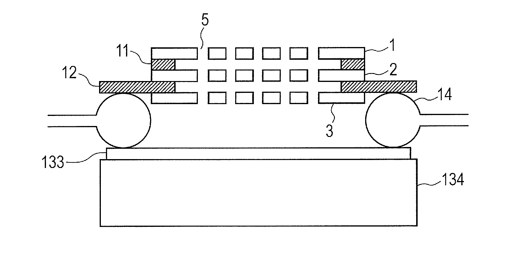
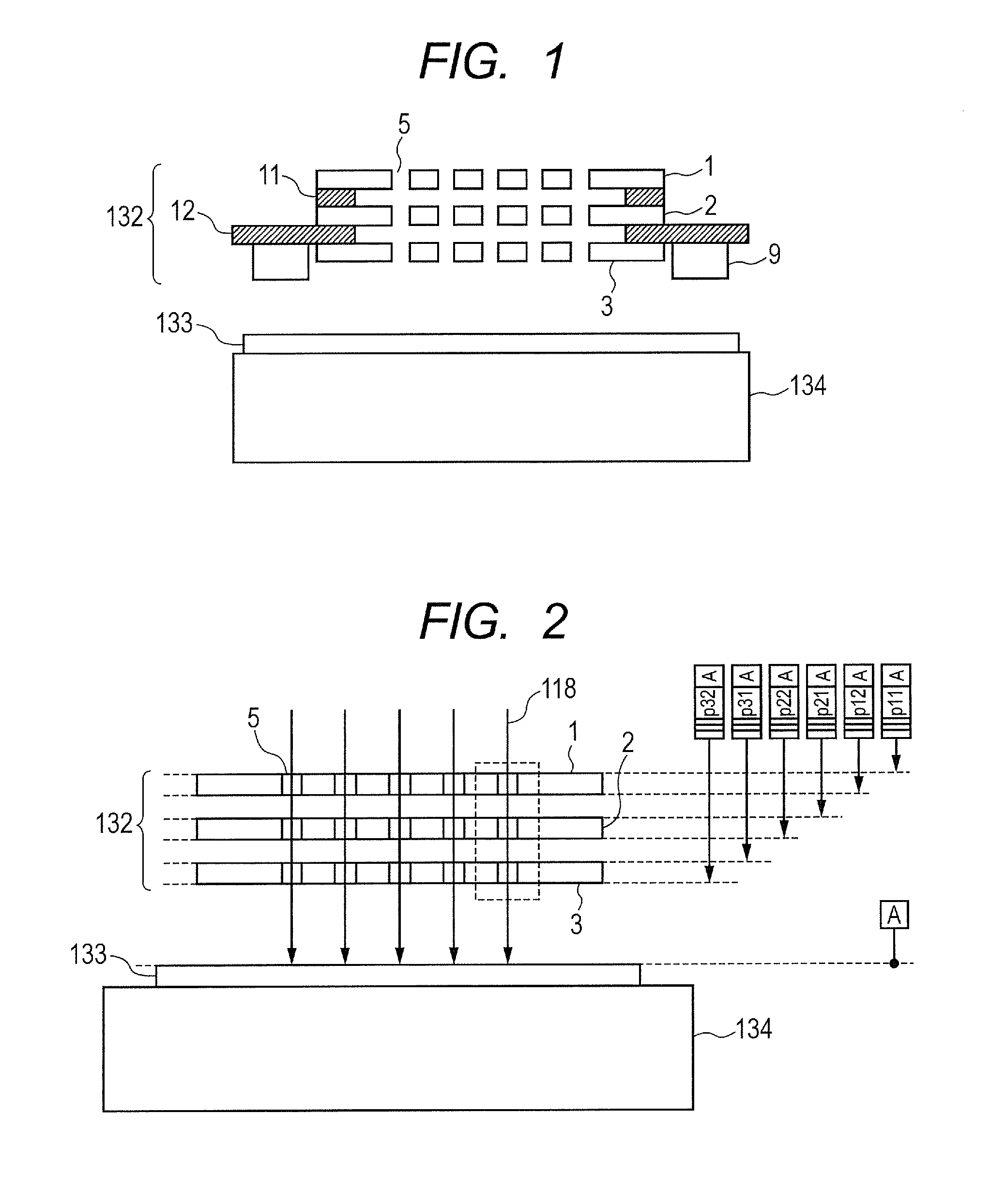
[0073]As Example 1, a structure example of an electrostatic lens array to which the present invention is applied is described with reference to FIG. 1.

[0074]FIG. 1 is a diagram illustrating details of the electrostatic lens array 132 illustrated in FIG. 10. An average thickness of each of the first electrode 1, the second electrode 2, and the third electrode 3 is 100 μm, and an average interval between the electrodes is 400 μm. Each electrode is made of metal or semiconductor.

[0075]An average diameter of the apertures 5 for passing the multiple electron beams is 30 μm, and an average distance between the surface of the wafer 133 and the lower surface of the electrostatic lens 132 is 100 μm.

[0076]Further, values of the thickness of the electrode, the interval between the electrodes, and the distance between the surface of the wafer 133 and the lower surface of the electrostatic lens 132 are not accurate but have errors of approximately ±1 μm, ±0.5 μm, and ±1 μm, respectively.

[0077]In...


PUM


Abstract

Provided is an electrostatic lens array, including multiple substrates arranged with intervals, each of the multiple substrates having an aperture for passing a charged particle beam, in which: in a travelling direction of the charged particle beam, a peripheral contour line formed by any one of surfaces of the multiple substrates other than an upper surface of a most upstream substrate and a lower surface of a most downstream substrate has a protruding portion protruding from a peripheral contour line of one of the upper surface of the most upstream substrate and the lower surface of the most downstream substrate; and a position of the protruding portion is defined by a position regulating member, whereby parallelism is adjustable so that a surface including the protruding portion is parallel to a surface to be irradiated with the charged particle beam after passing through the aperture.

Description

BACKGROUND OF THE INVENTION[0001]1. Field of the Invention[0002]The present invention relates to an electrostatic lens array that is used for a charged particle optical system.[0003]2. Description of the Related Art[0004]A multi-charged-particle beam drawing apparatus uses an electrostatic lens array for converging a charged particle beam (see Japanese Patent Application Laid-Open No. 2005-032480 and International Publication No. WO2011 / 043668). The multi-charged-particle beam drawing apparatus accelerates, shapes, and reduces charged particles emitted from a charged particle source, and irradiates a sample with the charged particle beam so as to draw a desired pattern on the sample. When shaping the charged particle beam, the electrostatic lens array is used for converging multiple charged particle beams separately.[0005]In the invention described in Japanese Patent Application Laid-Open No. 2005-032480, the electrostatic lens array is a lens for an image before a reducing optical ...

Claims


Application Information

Patent Timeline
Patent Type & Authority Patents(United States)
IPC IPC(8): G21K1/08
CPCH01J37/3177H01J37/12H01J2237/032H01J3/027G03F7/00H01J3/18H01J2237/1205H01J2237/28B82Y40/00B82Y10/00
Inventor OHASHI, YASUO
Owner CANON KK
Why Eureka
Try Eureka