Photoelectric detector with high bandwidth and high responsivity

A photodetector and responsivity technology, applied in the field of photodetectors, can solve the problems of complex manufacturing process of optical coupling lens, poor process repeatability, low product yield, etc., to achieve good responsivity, good convergence effect, easy focus and The effect of focal length

Active Publication Date: 2022-03-15
福建慧芯激光科技有限公司
View PDF8 Cites 1 Cited by
  • Summary
  • Abstract
  • Description
  • Claims
  • Application Information

AI Technical Summary

Problems solved by technology

However, the manufacturing process of the coupling lens is complex and difficult to control, the process repeatability is poor, and the product yield is low

Method used


Image

  • Photoelectric detector with high bandwidth and high responsivity
  • Photoelectric detector with high bandwidth and high responsivity
  • Photoelectric detector with high bandwidth and high responsivity

Examples


Embodiment approach

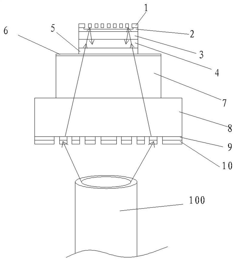
[0038] refer to Figure 4 , as an embodiment of the present invention, a spacer layer 9 is also provided between the InP substrate 8 and the second grating layer 10, the shape of the spacer layer 9 matches the annular grating strip, the spacer layer 9 is made of InAlAs, and the thickness is At 180-600nm, the spacer layer 9 is finally oxidized, and the main component is Al with low refractive index. 2 o 3 .

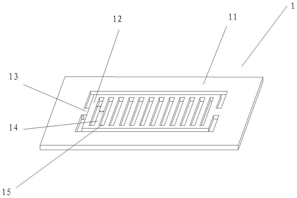
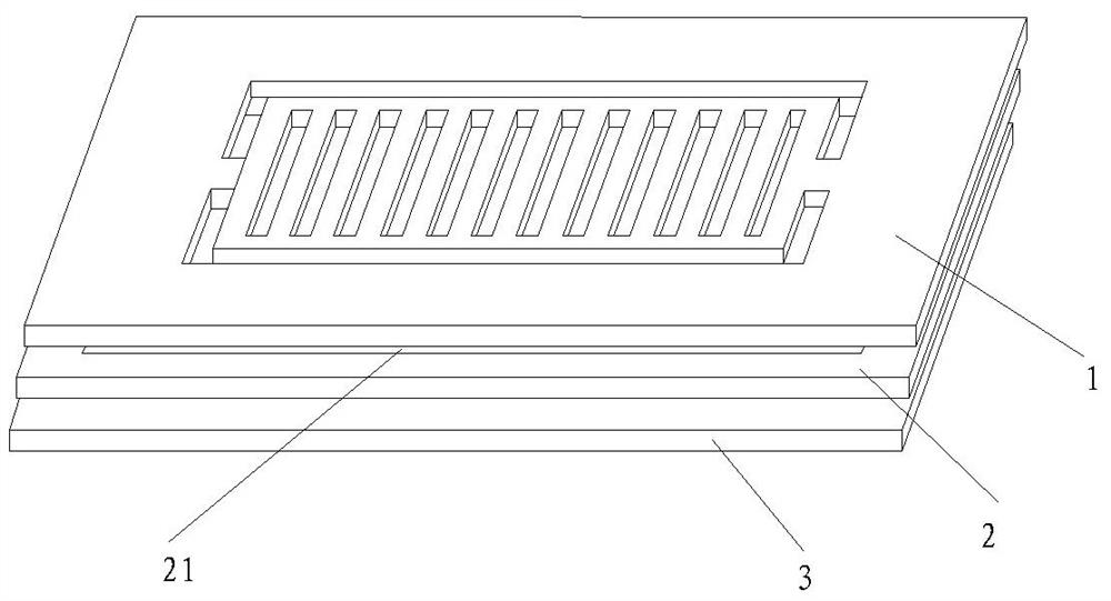
[0039] refer to Figure 6 , in another embodiment of the second grating layer 10 of the present invention, its difference from the above-mentioned structure is that: the second grating layer 10 is provided with a round hole, and a plurality of grating bars are arranged in the round hole, and a plurality of The grating strips are arranged in parallel, the widths of each grating strip are not all the same or the gaps between adjacent grating strips are not all the same, a spacer layer 9 is provided between the second grating layer 10 and the substrate 8, and the spacer la...


PUM

PropertyMeasurementUnit
thicknessaaaaaaaaaa
diameteraaaaaaaaaa
thicknessaaaaaaaaaa

Abstract

The invention relates to a photoelectric detector with high bandwidth and high responsivity, which belongs to the field of semiconductor devices and comprises an InP substrate, and an InP isolation table, an N-type contact layer, an N-type InP layer, an InGaAs light absorption layer, a P-type InP layer and a P-type contact layer which are sequentially grown on the InP substrate, the device is characterized in that a first grating layer used for reflecting light emitted by the P-type contact layer to the InGaAs light absorption layer is arranged on the P-type contact layer, a second grating layer used for converging, transmitting and automatically coupling light beams is arranged on one side, back to the InP isolation platform, of the InP substrate, the second grating layer comprises a plurality of annular grating strips which are concentrically arranged, the diameter of the InGaAs light absorption layer is 5-10 m, and the diameter of the InGaAs light absorption layer is 5-10 m. And the thickness is 500 to 3000 nm. According to the invention, the PD bandwidth can be improved, and the PD responsivity can be improved and the PD light coupling difficulty can be reduced at the same time.

Description

technical field [0001] The invention relates to a photodetector with high bandwidth and high responsivity. Background technique [0002] A photodetector (PD) is a device that converts light signals into electrical signals. The development of 5G communication, data center / cloud computing, Internet of Things and smart cities has made optical information and optical network a national strategic information infrastructure. Optical modules are the core of optical information and optical networks. The optical chip is the core component of the optical module, and its value accounts for nearly 50% of the cost of the optical module / optical device. With the improvement of the performance index of the optical module, it occupies the commanding heights of the value of the entire industry chain and is the "high value" of the optical device. Pearl". PD is generally used in conjunction with VCSEL and DFB, and is mainly used in industrial fields such as the telecom market, data center ma...

Claims


Application Information

Patent Timeline
Patent Type & Authority Applications(China)
IPC IPC(8): H01L31/0232H01L31/10H01L31/105
CPCH01L31/02327H01L31/10H01L31/105
Inventor 鄢静舟王坤薛婷杨奕
Owner 福建慧芯激光科技有限公司
Why Eureka
Try Eureka