Dielectric covered planar antennas

a planar antenna and dielectric technology, applied in the field of imaging planar antennas, can solve the problems of limiting the size of such an array design, difficult fabrication using such designs,

Active Publication Date: 2014-07-15
CALIFORNIA INST OF TECH
View PDF11 Cites 225 Cited by
  • Summary
  • Abstract
  • Description
  • Claims
  • Application Information

AI Technical Summary

Problems solved by technology

Furthermore, multimode corrugated feed horns have also shown very good pattern characteristics, although fabrication becomes difficult using such designs for very large focal planes at high frequencies.
However, most planar antenna designs produce broad beam patterns, and therefore require additional elements for efficient coupling to the telescope optics, such as substrate lenses or micro-machined horns.
Although this does not necessarily preclude their use in large arrays, and indeed large arrays using substrate lenses are being investigated; the key issues for such development include resolving the manufacture and assembly of a large “fly's eye” array of lenses.
While it is also possible to place an array of antennas behind a single lens, optical aberrations tend to limit the size of such an array design.

Method used


Image

  • Dielectric covered planar antennas
  • Dielectric covered planar antennas
  • Dielectric covered planar antennas

Examples


Embodiment Construction

[0033]1. Overview

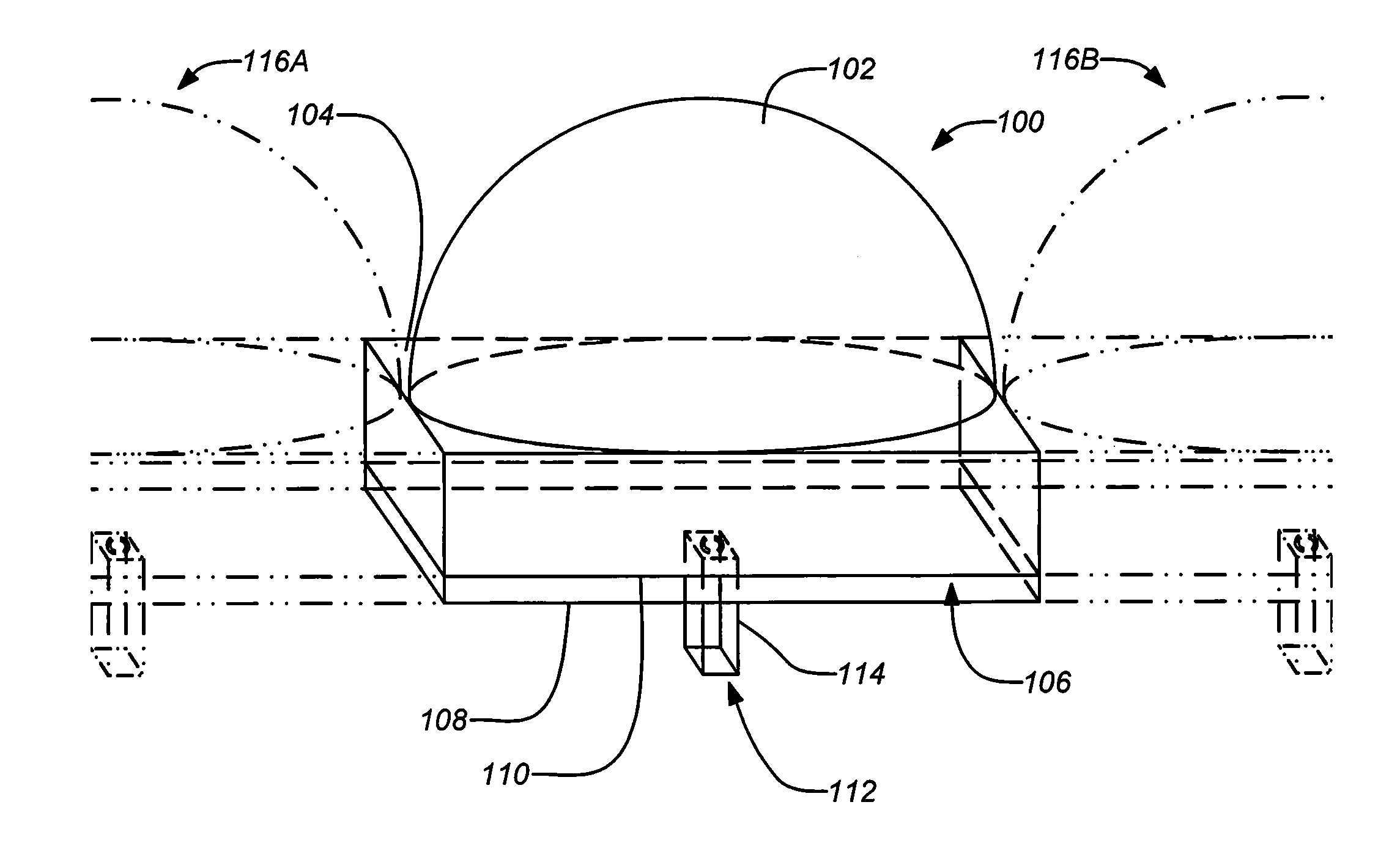
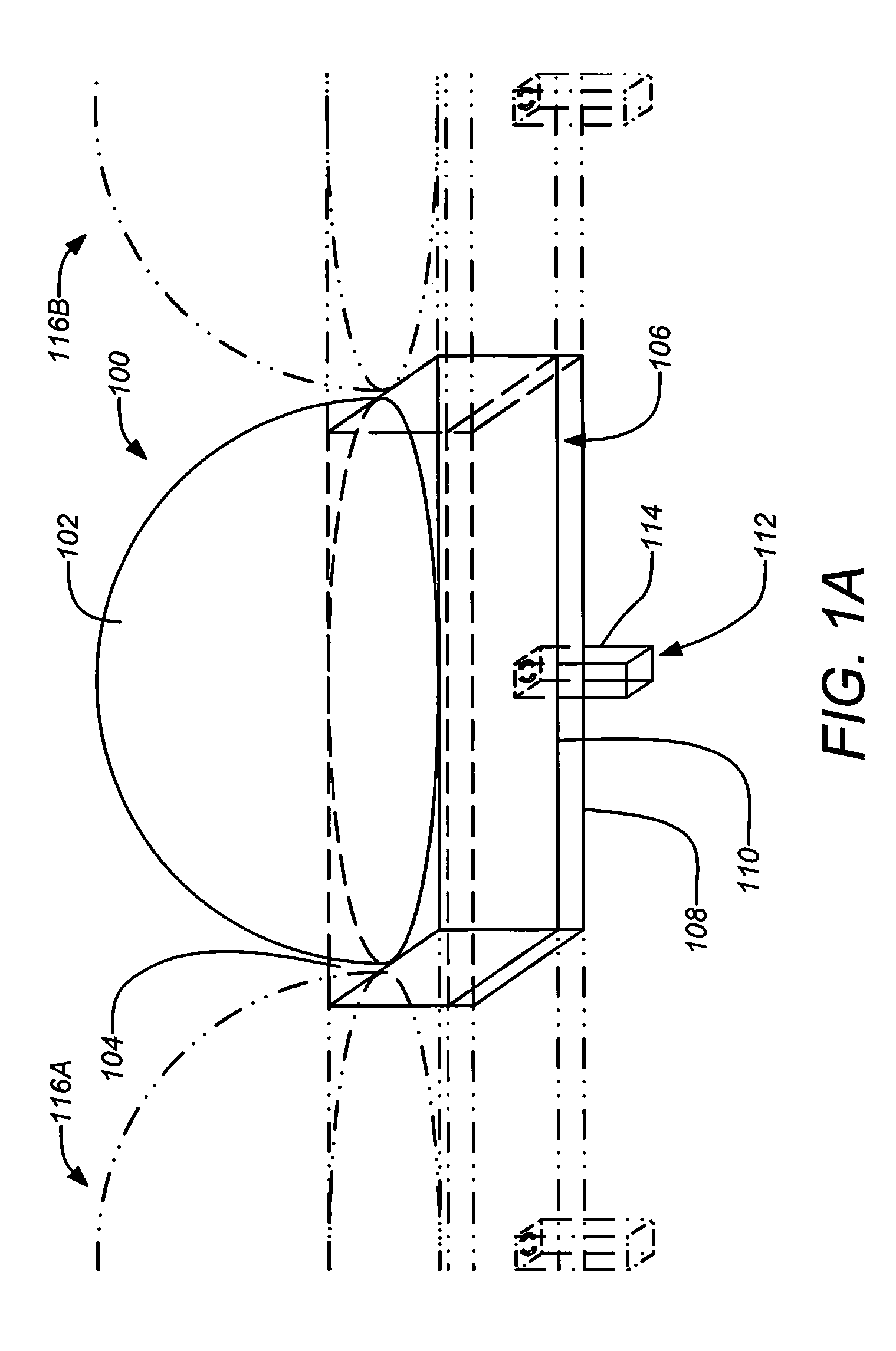
[0034]As mentioned above, embodiments of the present invention are direct to a novel antenna suitable for integrated arrays at terahertz frequencies. The antenna may include a waveguide feed, which can be integrated with Schottky detectors and mixers, that excites a silicon lens antenna through a leaky-wave or electromagnetic band-gap (EBG) resonant cavity. The cavity is used to both match the waveguide feed with the silicon medium and to illuminate the upper part of the lens.

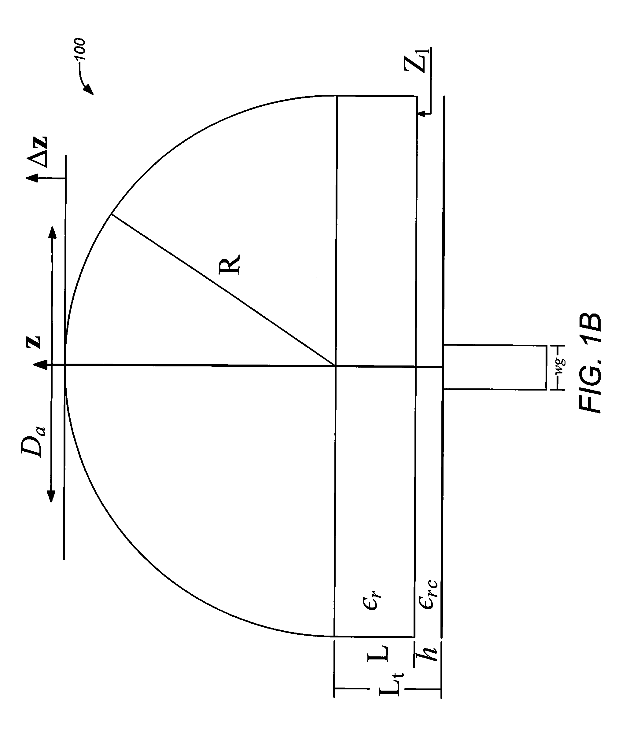
[0035]Embodiments of the invention effectively address the issues described above by using an integrated silicon micro lens which can potentially be fabricated using photolithographic techniques. See e.g., Lee et al., “A glass reflowed microlens array on a Si substrate with rectangular through-holes,” J. Opt. A. 10 (2008) 044003, 2008, which is incorporated by reference herein. Example embodiments of the invention may employ an extended hemispherical lens antenna fed by a leaky wave feed. The p...


PUM


Abstract

An antenna element suitable for integrated arrays at terahertz frequencies is disclosed. The antenna element comprises an extended spherical (e.g. hemispherical) semiconductor lens, e.g. silicon, antenna fed by a leaky wave waveguide feed. The extended spherical lens comprises a substantially spherical lens adjacent a substantially planar lens extension. A couple of TE / TM leaky wave modes are excited in a resonant cavity formed between a ground plane and the substantially planar lens extension by a waveguide block coupled to the ground plane. Due to these modes, the primary feed radiates inside the lens with a directive pattern that illuminates a small sector of the lens. The antenna structure is compatible with known semiconductor fabrication technology and enables production of large format imaging arrays.

Description

CROSS-REFERENCE TO RELATED APPLICATIONS[0001]This application claims the benefit under 35 U.S.C. §119(e) of the following U.S. provisional patent application, which is incorporated by reference herein:[0002]U.S. Provisional Patent Application No. 61 / 221,695, filed Jun. 30, 2009, and entitled “DIELECTRIC COVERED PLANAR ANTENNAS AT SUBMILLIMETER WAVELENGTHS FOR TERAHERTZ IMAGING APPLICATIONS”, by Gill et al.STATEMENT OF GOVERNMENT RIGHTS[0003]The invention described herein was made in the performance of work under a NASA contract, and is subject to the provisions of Public Law 96-517 (35 U.S.C. 202) in which the Contractor has elected to retain title.BACKGROUND OF THE INVENTION[0004]1. Field of the Invention[0005]This invention relates to imaging planar antennas. Particularly, this invention relates to dielectric covered planar antennas for terahertz imaging applications.[0006]2. Description of the Related Art[0007]Large focal planes employing thousands of detectors are expected to be...

Claims


Application Information

Patent Timeline
Patent Type & Authority Patents(United States)
IPC IPC(8): H01Q19/06
CPCH01Q19/09G01N21/3581H01Q19/06H01Q21/06
Inventor LLOMBART JUAN, NURIALEE, CHOONSUPCHATTOPADHYAY, GOUTAMGILL, JOHN J.SKALARE, ANDERS J.SIEGEL, PETER H.
Owner CALIFORNIA INST OF TECH
Why Eureka
Try Eureka