Non-volatile memory

a non-volatile memory and memory technology, applied in the direction of semiconductor devices, electrical equipment, transistors, etc., can solve the problems of easy program disturbance, affecting operation window and device performance,

Active Publication Date: 2014-07-29
MACRONIX INT CO LTD
View PDF7 Cites 0 Cited by
  • Summary
  • Abstract
  • Description
  • Claims
  • Application Information

AI Technical Summary

Benefits of technology

[0008]The embodiment of the invention provides a manufacturing method of a non-volatile memory capable of manufacturing a non-volatile memory that can prevent from generating second bit effect and program disturbance in operation.
[0009]The embodiment of the invention further provides a non-volatile memory capable of preventing the generation of second bit effect and program disturbance in operation.
[0028]In light of the foregoing, the charge storage spacers formed on the sidewalls of the oxide protrusion is adopted as the charge storage regions in the invention. The charges are thus respectively confined in the charge storage spacers effectively to prevent the second bit effect during the read operation and prevent the program disturbance of adjacent memory cells during the program operation. Further, by adjusting the thickness of the charge storage material layer in the invention, the size of the charge storage spacers formed therefrom can be controlled to prevent the size of the charge storage spacers from being too small which in term affects the ability of the memory to store charges.

Problems solved by technology

Also, with the reduction in the size of memory, the length of the channel in the memory cell is reduced as well, such that the second bit effect is more severe, thereby affecting operation window and device performance.
Consequently, program disturbance easily results when adjacent memory cells undergo a program operation.

Method used


Image

  • Non-volatile memory
  • Non-volatile memory
  • Non-volatile memory

Examples


first embodiment

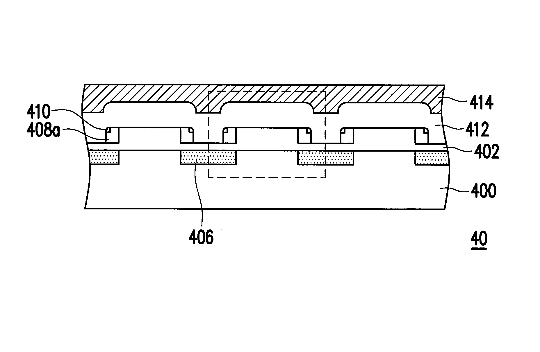
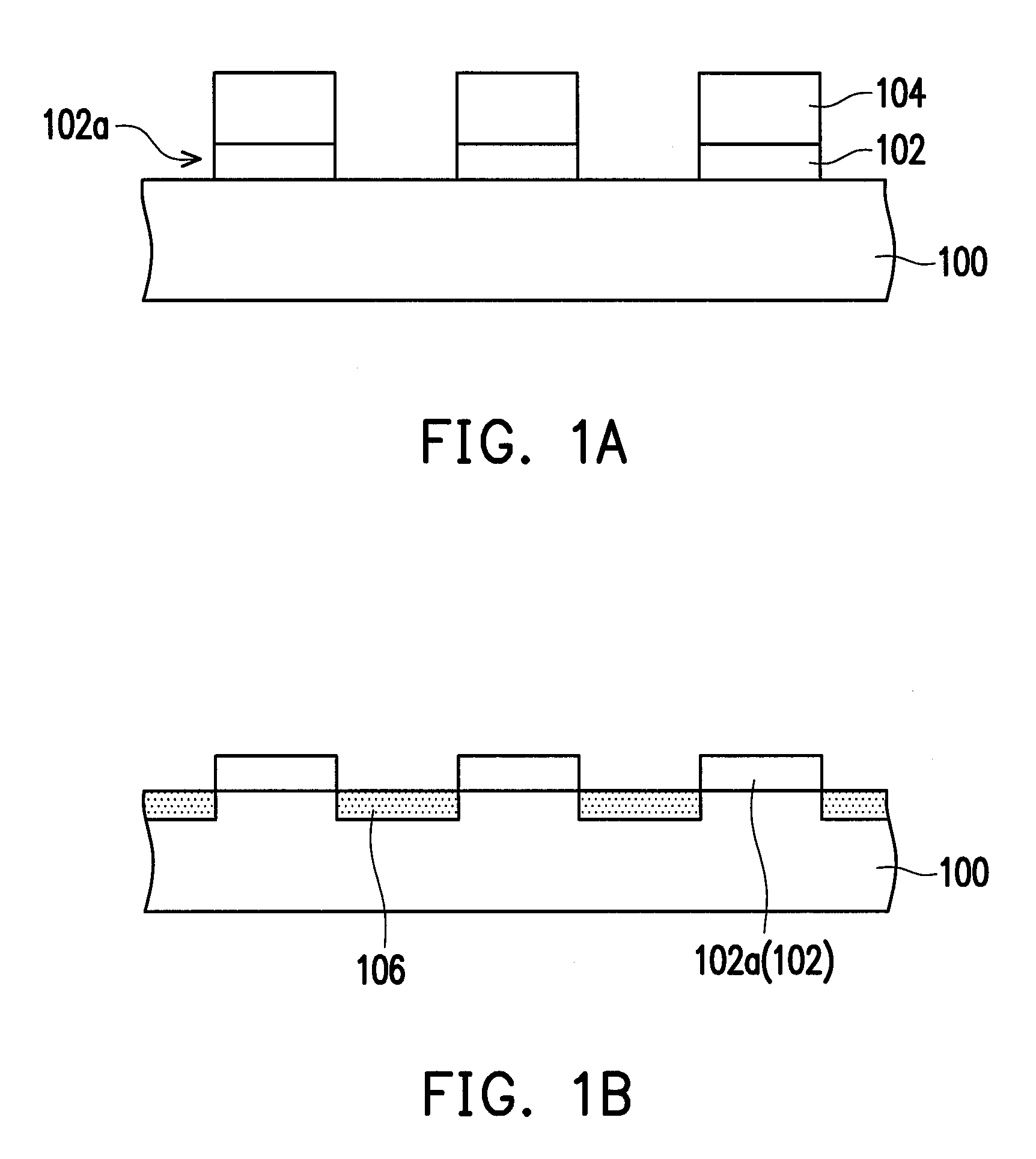
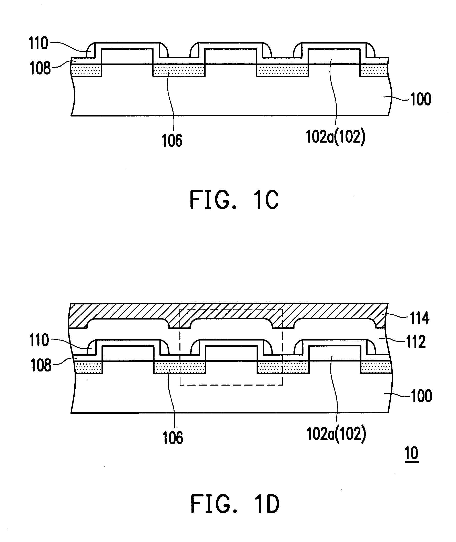
[0036]FIGS. 1A to 1D are schematic cross-sectional diagrams showing a flowchart for manufacturing a non-volatile memory according to a first embodiment of the invention. Referring to FIG. 1A, an oxide layer 102 having a protrusion 102a is formed on a substrate 100. The oxide layer 102 is formed by forming an oxide material layer on the substrate 100, for example. A method of forming the oxide material layer is, for example, a chemical vapor deposition (CVD) method. Thereafter, a patterning mask layer 104 is formed on the oxide material layer. The patterning mask layer 104 covers a region for forming the protrusion in the oxide layer 102. Afterwards, the patterning mask layer 104 is used as a mask to perform an isotropic etching process so as to remove a portion of the oxide material layer until the substrate 100 is exposed to form the protrusions 102a. In the present embodiment, since the oxide layer 102 not covered by the patterning mask layer 104 is removed, the oxide layer 102 re...

second embodiment

[0042]FIGS. 2A to 2C are schematic cross-sectional diagrams showing a flowchart for manufacturing a non-volatile memory according to a second embodiment of the invention. Referring to FIG. 2A, an oxide layer 202 having a protrusion 202a is formed on a substrate 200. The oxide layer 202 is formed by forming an oxide material layer on the substrate 200, for example. A method of forming the oxide material layer is, for example, a CVD method. Thereafter, a patterning mask layer 204 is formed on the oxide material layer. The patterning mask layer 204 covers a region for forming the protrusion in the oxide layer 202. Afterwards, the patterning mask layer 204 is used as a mask to perform an isotropic etching process so as to remove a portion of the oxide material layer without exposing the substrate 200 to form the protrusions 202a.

[0043]Referring to FIG. 2B, the patterning mask layer 204 is adopted as a mask to perform an ion implantation process so as to form a pair of doped regions 206...

third embodiment

[0046]FIGS. 3A to 3D are schematic cross-sectional diagrams showing a flowchart for manufacturing a non-volatile memory according to a third embodiment of the invention. Referring to FIG. 3A, an oxide layer 302 having a protrusion 302a is formed on a substrate 300. The oxide layer 302 is formed by forming an oxide material layer on the substrate 300, for example. A method of forming the oxide material layer is, for example, a CVD method. Thereafter, a patterning mask layer 304 is formed on the oxide material layer. The patterning mask layer 304 covers a region for forming the protrusion in the oxide layer 302. Afterwards, the patterning mask layer 304 is used as a mask to perform an isotropic etching process so as to remove a portion of the oxide material layer without exposing the substrate 300 to form the protrusions 302a.

[0047]Referring to FIG. 3B, a pair of nitride spacers 306 is formed on the sidewalls of the patterning mask layer 304 and the protrusions 302a. A method of form...


PUM


Abstract

A non-volatile memory and a manufacturing method thereof are provided. A first oxide layer having a protrusion is formed on a substrate. A pair of doped regions is formed in the substrate at two sides of the protrusion. A pair of charge storage spacers is formed on the sidewalls of the protrusion. A second oxide layer is formed on the first oxide layer and the charge storage spacers. A conductive layer is formed on the second oxide layer.

Description

BACKGROUND OF THE INVENTION[0001]1. Field of the Invention[0002]The invention relates to a non-volatile memory (NVM) and a manufacturing method thereof. More particularly, the invention relates to a non-volatile memory capable of preventing second bit effect and program disturbance and a manufacturing method thereof.[0003]2. Description of Related Art[0004]Non-volatile memory has the advantage of saving the stored data after the power is turned off. Thus, this type of memory is adopted in many electronic products to maintain the operation of electronic products when turned on.[0005]Nitride read only memory (ROM) is a common non-volatile memory nowadays. In a memory cell of a nitride ROM, a charge trapping structure constituted by a nitride layer can store two-bit data. Generally, two-bit data can be stored in the left side (that is, left bit) and the right side (that is, right bit) of the charge trapping structure respectively.[0006]However, two bit effect is present in the nitride ...

Claims


Application Information

Patent Timeline
Patent Type & Authority Patents(United States)
IPC IPC(8): H01L29/792
CPCH01L29/7923H01L29/66833H01L29/7887H01L29/42332H01L27/11568H01L29/42336H01L27/11521H01L29/66825H10B43/30H10B41/30
Inventor CHENG, CHIH-CHIEHYAN, SHIH-GUEICHENG, CHENG-HSIENTSAI, WEN-JER
Owner MACRONIX INT CO LTD
Why Eureka
Try Eureka