Light emitting device

a technology of light-emitting devices and light-emitting components, which is applied in the direction of semiconductor devices, electrical equipment, basic electric elements, etc., can solve the problems of insufficient light-emitting efficiency, and achieve the effect of improving the utilization efficiency of light-emitting components and low substrate cos

Inactive Publication Date: 2014-09-02
SUMITOMO ELECTRIC IND LTD
View PDF32 Cites 0 Cited by
  • Summary
  • Abstract
  • Description
  • Claims
  • Application Information

AI Technical Summary

Benefits of technology

[0007]According to the aspect of the present invention, the light emitting device can emit light produced by superposition of a light component emitted from the light emitting layer and a light component induced by a light component incident on the base from the light emitting layer. Because an angle between the c-axis of the gallium nitride layer and the normal line to the principal surface of the gallium nitride layer is in a range of not less than 50 degree and not more than 130 degree, indium content in the light emitting layer is relatively high, and thus, it allows for emission of high-intensity light. Because the angle between the c-axis of the gallium nitride layer and the normal line to the principal surface of the gallium nitride layer is in a range of not less than 50 degree and not more than 130 degree, the piezoelectric field is relatively weak, and thus, it allows for a relatively smaller variation width in wavelength of light from the light emitting layer which is induced by a variation in drive current. The absolute value of the degree of polarization of not less than 0.2 indicates a relatively high degree of polarization.
[0009]The light emitting device further comprising a reflective layer which is disposed on the back surface of the phosphor layer, the reflective layer reflecting light which is emitted from the phosphor layer. Therefore, it allows for an improvement in utilization efficiency of light incident on the phosphor layer.
[0010]In the light emitting device, the gallium nitride layer has a thickness in a range of not less than 100 nm and not more than 1200 nm. Therefore, it allows for compatibility of high-quality and low cost of the substrate.

Problems solved by technology

However, because of insufficient polarization properties, insufficient light emitting efficiency, complexity of configuration, or the like, a light emitting device having a relatively simple configuration and exhibiting sufficient polarization properties and sufficient light emitting efficiency is desired.

Method used


Image

  • Light emitting device
  • Light emitting device
  • Light emitting device

Examples


Embodiment Construction

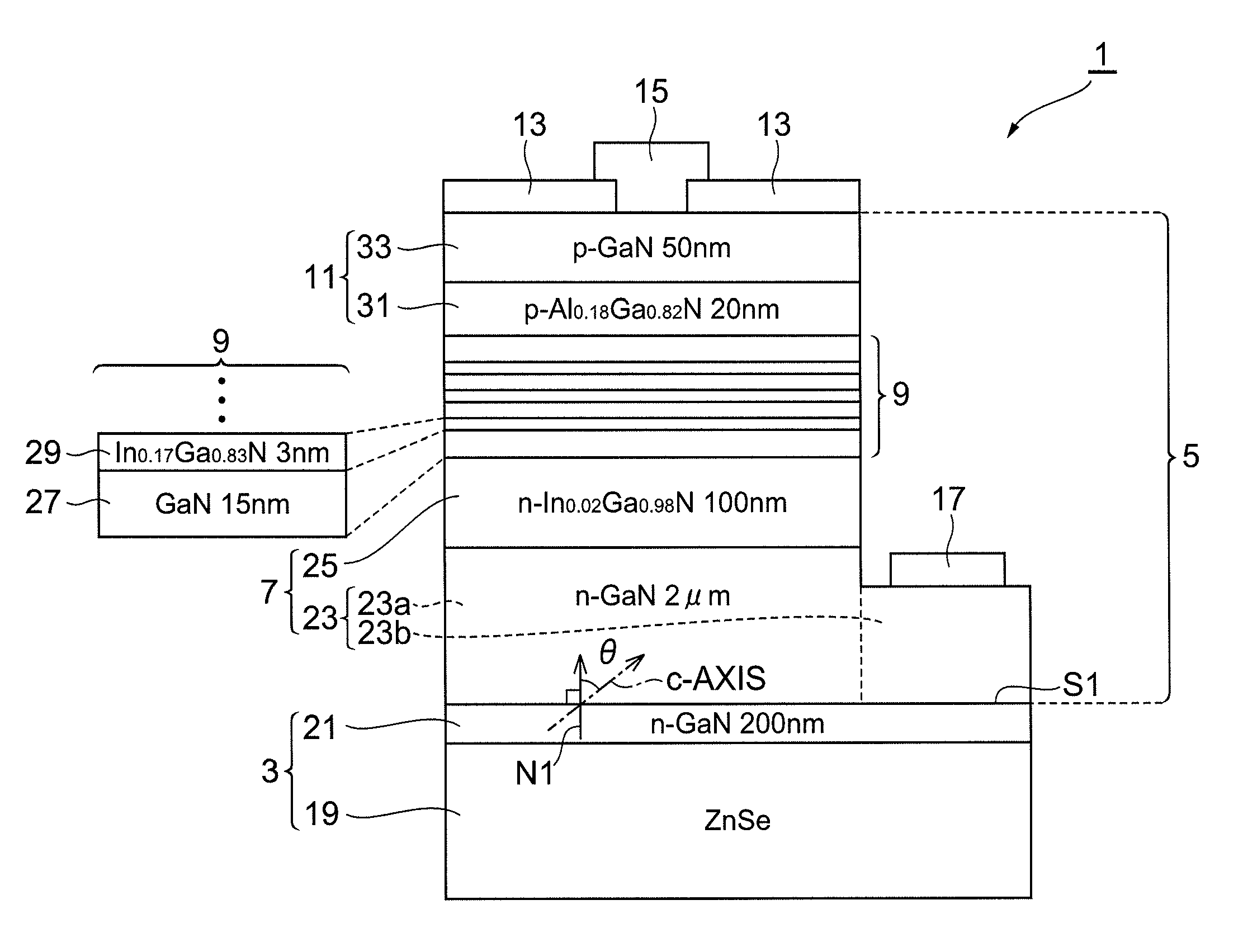
[0018]Preferred embodiments according to the present invention will be described with reference to the attached drawings. In order to avoid redundancy in description of the drawings, the same elements are designated by the same reference numerals, wherever possible. In FIG. 1, a configuration of a light emitting device 1 according to the embodiment is shown. The light emitting device 1 comprises a composite substrate 3, a gallium nitride-based semiconductor layer 5, a p-electrode 13, a pad electrode 15, and an n-electrode 17. The composite substrate 3 includes a base 19 and a GaN layer 21. The base 19 contains a fluorescent material that emits a fluorescent light component induced by irradiation of a light component emitted from a light emitting layer 9 as described below. The fluorescent material contains a component that emits yellow light having a peak wavelength in a range of not less than 540 nm and not more than 600 nm by absorbing blue light having a peak wavelength in a rang...


PUM


Abstract

A light emitting device having a relatively simple configuration is provided that emits stable light having a plurality of wavelengths. The light emitting device 1 comprises, in sequence, a composite substrate 3 and a gallium nitride-based semiconductor layer 5 including a light emitting layer 9. The composite substrate 3 includes a base 19 and a gallium nitride layer, the gallium nitride-based semiconductor layer 5 being disposed on a principal surface of the gallium nitride layer, the angle θ defined by the c-axis of the gallium nitride layer and a normal line N1 to the principal surface S1 of the gallium nitride layer ranging from 50 to 130 degrees, the light emitting layer 9 emitting light with an absolute value of the degree of polarization of 0.2 or more, the base 19 containing a fluorescent material that emits a fluorescent light component induced by irradiation of a light component emitted from the light emitting layer 9. Accordingly, the light emitting device 1 can emit white light produced by superposition of blue light directly emitted from the light emitting layer 9 and yellow light induced by blue light incident on the base 19 from the light emitting layer 9.

Description

BACKGROUND OF THE INVENTION[0001]1. Field of the Invention[0002]The present invention relates to a light emitting device.[0003]2. Related Background Art[0004]In recent years, light emitting devices that emit light having a plurality of wavelengths (colors) have been developed. Patent Literature 1 (Japanese Unexamined Patent Application Publication No. 2008-159606) discloses a nitride semiconductor light emitting device comprising a GaN semiconductor layer formed on a GaN substrate, the GaN semiconductor layer including a first and second quantum well layers that emit light having different wavelengths. A color mixture of colors of light components emitted from the first and second active layers is observed. Patent Literature 2 (Japanese Unexamined Patent Application Publication No. 2008-218645) discloses a light emitting device comprising a blue light emitting diode chip and a yellow light emitting diode chip that are mounted on a supporting substrate, thereby producing white light ...

Claims


Application Information

Patent Timeline
Patent Type & Authority Patents(United States)
IPC IPC(8): H01L33/32H01L33/50H01L33/08
CPCH01L33/08H01L33/32H01L33/16
Inventor KYONO, TAKASHI
Owner SUMITOMO ELECTRIC IND LTD
Why Eureka
Try Eureka