Substrate for use in preparing solar cells

a solar cell and substrate technology, applied in the field of photoelectric devices, can solve the problems of bowing damage to silicon wafers, cracking of silicon wafers, and clogging of silicon wafers used as solar cells, and achieve the effects of reducing the overall cte of composite materials, reducing the adverse effects of bowing from cte mismatch, and high conductivity of aluminum

Inactive Publication Date: 2014-09-09
MOSSEY CREEK TECH
View PDF34 Cites 3 Cited by
  • Summary
  • Abstract
  • Description
  • Claims
  • Application Information

AI Technical Summary

Benefits of technology

[0015]Disclosed herein are methods and processes for fabricating photoelectric devices and more particularly to methods and processes for fabricating a conductive back face substrate for silicon wafer solar cells. In many embodiments of the present invention, a conductive material, such as aluminum, is combined with other substances having lower CTE to form a composite material for use as a back face substrate. This composite material takes advantage of the high conductivity of aluminum, while the other substances reduce the overall CTE of the composite material and thereby diminish the adverse effects of bowing from CTE mismatch. In at least one embodiment of the present invention, a conductive composite substrate material is fabricated by mixing particulate aluminum with a particulate additive comprising a mineral, ceramic, or other small particulate with a low CTE, and casting and firing the mixture so that the aluminum forms a continuous phase that will be electrically conductive, and the additive forms a discontinuous phase that will control and match the CTE of the mixture to be equal to or close to that of silicon. In several embodiments, the additive is a material with a high temperature melting point, a small particle size, and a low CTE. In several embodiments, the additive is co-milled with or mixed into a fine aluminum powder in order to make a castable or shapeable precursor or body, which can be shaped into a back face substrate, wherein the low CTE particles become the discontinuous phase in the back face substrate. This body is then fired to the melting point of aluminum, at which point, upon solidification, the additive particles, which are very strong in compression, are put into compression as the aluminum seeks to shrink, causing the aluminum to build up tensile stresses which are relieved by elongation. In several embodiments, by tailoring the distribution of particle sizes and amount of volume filled with the low CTE particles, a conductive aluminum-based back face substrate member is made having a tailored CTE essentially close to that of silicon.

Problems solved by technology

Significant bowing can damage a silicon wafer, for example by leading to separation between the silicon layer of the solar cell and the back face substrate, or by causing the silicon wafer to crack.
In addition to bowing during the fabrication process, a silicon wafer used as a solar cell may also experience bowing due to changes in temperature during use.
In particular, a silicon wafer solar cell should be designed to withstand exceptionally low winter temperatures, which may be infrequent but can nevertheless cause failures such as those discussed above when they do occur.
However, this class of substrate materials is generally ill-suited for use in a solar cell because the ceramic materials with a low CTE close to the CTE of silicon are generally insulators and are poor electrical conductors.
However, essentially all of the candidate metals have a high mismatch of CTE as compared to silicon.
Gold and platinum have high melting points and would present high material costs for use in silicon wafers.
Silver has a slightly lower melting point, but silver's lack of elongation and relatively high cost also make it impractical to use as a substrate material for a conducting back face substrate.
However, Aluminum by itself as a substrate presents the possibility of significant bowing because of the great difference in CTE between silicon (which is approximately 3 parts per million per degree Celsius) and aluminum (which is approximately 23 parts per million per degree Celsius).

Method used


Image

  • Substrate for use in preparing solar cells
  • Substrate for use in preparing solar cells
  • Substrate for use in preparing solar cells

Examples


Embodiment Construction

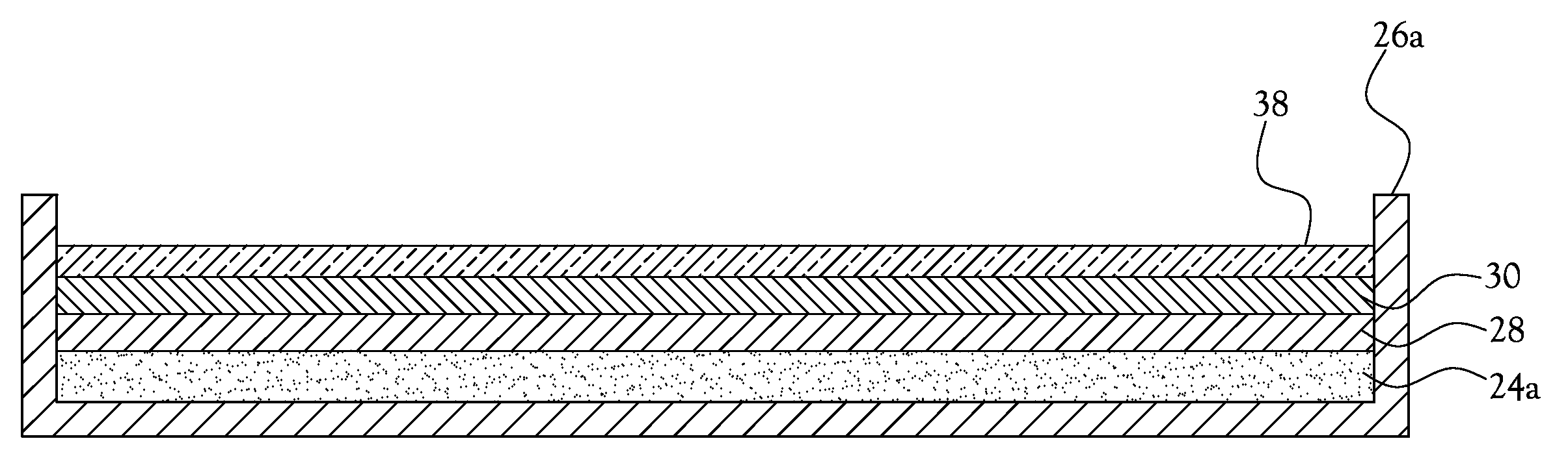
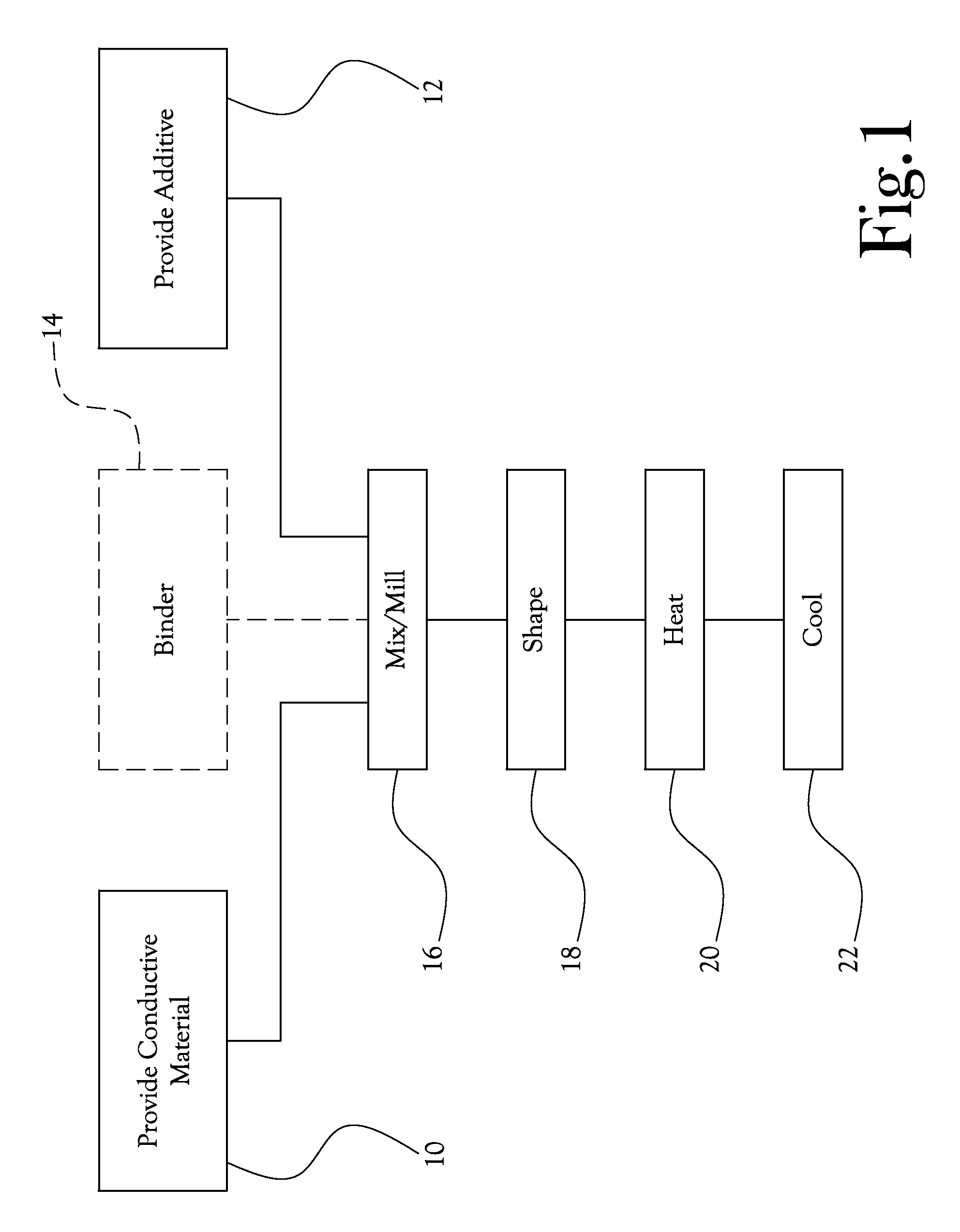
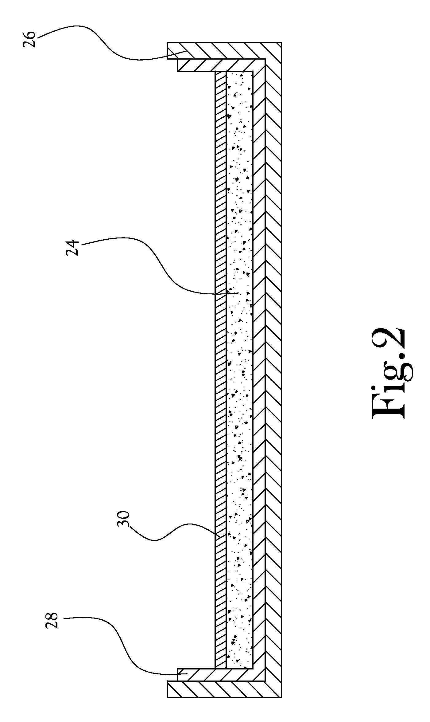
[0022]Disclosed herein are methods and processes for fabricating photoelectric devices, and more particularly, methods and processes for fabricating a back face substrate for a silicon wafer solar cell. In several embodiments, the methods and processes of the present general inventive concept provide for the manufacture of a back face substrate for a silicon wafer solar cell having a relatively high conductivity, and also having a relatively low CTE. According to several features of the present general inventive concept, a back face substrate is provided which includes a finely divided particulate additive bonded in a continuous phase of conductive material, the particulate additive imparting a low CTE to the back face substrate while the continuous phase of conductive material maintains conductivity of the back face substrate. In many embodiments of the present invention, a continuous phase of the back face substrate is provided which comprises aluminum or other such conductive mat...


PUM

PropertyMeasurementUnit
particle sizeaaaaaaaaaa
thicknessaaaaaaaaaa

Abstract

Conductive material is combined with other substances to form a composite material for use as a conductive back face substrate for a thin silicon wafer solar cell. In at least one embodiment, a conductive composite substrate material is fabricated by filling granular conductive material with a mineral or ceramic or other small particulate with a low CTE; the composite is cast and fired so that it has an electrically conductive continuous phase and a discontinuous phase that will control and match the CTE of the substrate to be equal to or close to that of silicon, thereby diminishing the effects of bowing from CTE-mismatch.

Description

CROSS-REFERENCE TO RELATED APPLICATIONS[0001]This application claims the benefit of U.S. Provisional Patent Application No. 61 / 509,618, filed on Jul. 20, 2011, which is incorporated herein in its entirety by reference.STATEMENT REGARDING FEDERALLY SPONSORED RESEARCH OR DEVELOPMENT[0002]Not ApplicableBACKGROUND OF THE INVENTION[0003]1. Field of Invention[0004]The present invention relates to methods and processes for fabricating photoelectric devices, and more particularly to methods and processes for fabricating the back face substrate for silicon wafer solar cells.[0005]2. Description of the Related Art[0006]In most current embodiments of solar cell technology, a solar cell comprises a silicon wafer built on a substrate (the “back face substrate”). In this respect, a silicon wafer solar cell closely resembles other silicon wafer semiconductor devices. Accordingly, certain methods and technologies used to fabricate silicon wafers for use in conventional semiconductor devices are als...

Claims


Application Information

Patent Timeline
Patent Type & Authority Patents(United States)
IPC IPC(8): H01L21/00
CPCH01L31/1804Y02E10/547Y02P70/50
Inventor CARBERRY, JOHN
Owner MOSSEY CREEK TECH
Why Eureka
Try Eureka