

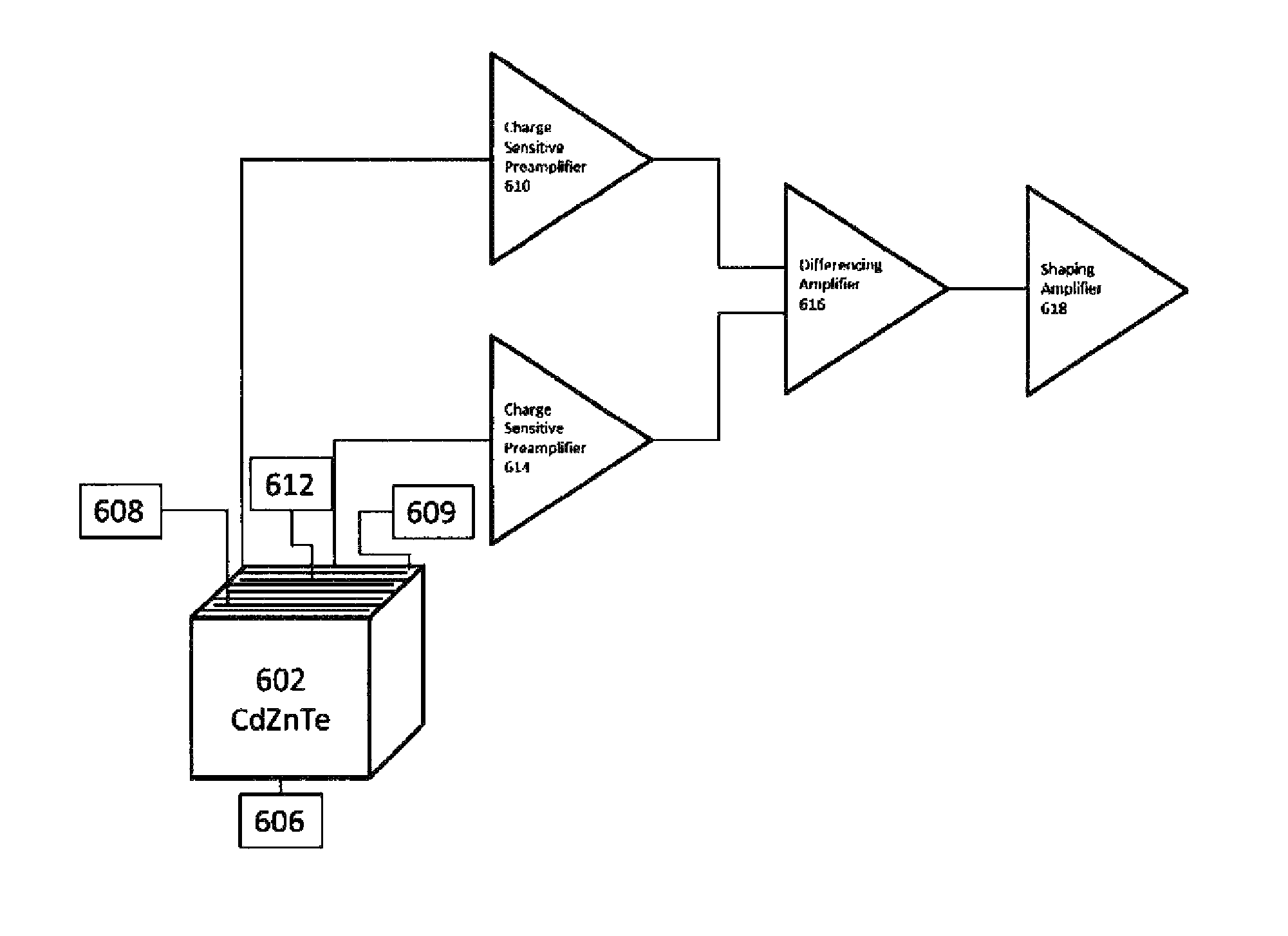
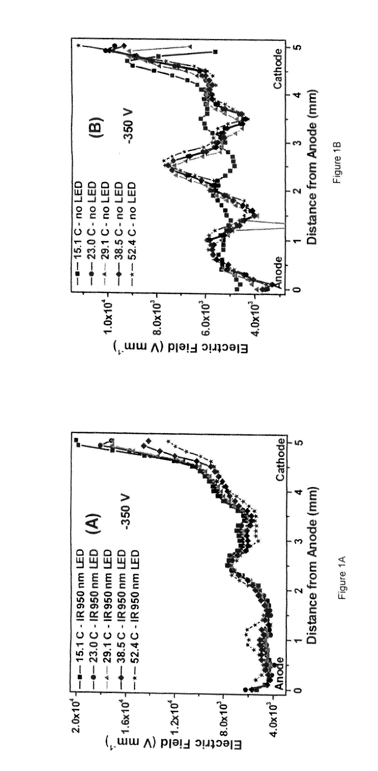
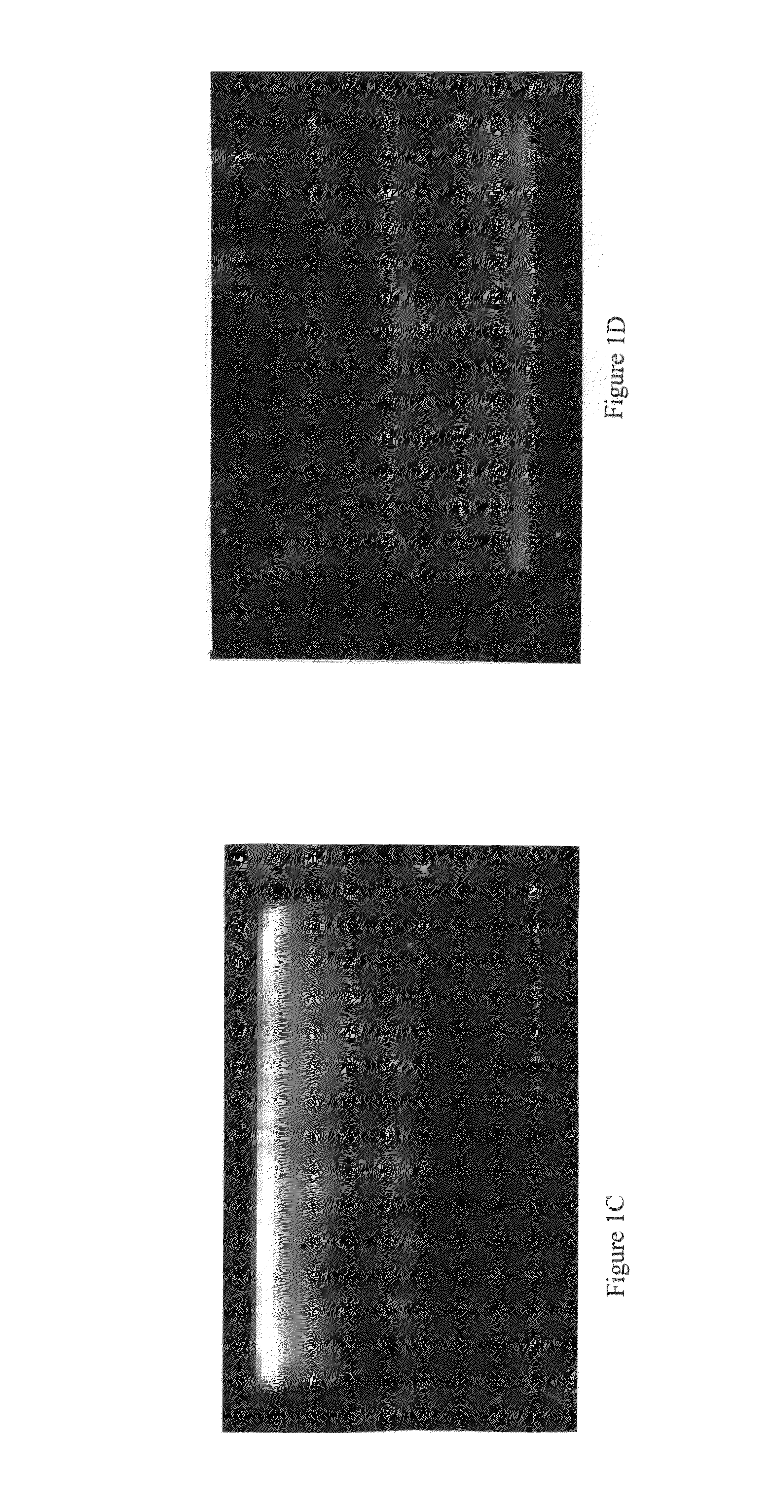
Modification of solid state CdZnTe (CZT) radiation detectors with high sensitivity or high resolution operation
a gamma radiation and detector technology, applied in the direction of optical radiation measurement, radiation controlled devices, instruments, etc., can solve the problems of affecting the birefringence of the czt crystal, and the change of the internal electric field of the crystal, so as to improve the charge collection capability
- Summary
- Abstract
- Description
- Claims
- Application Information
AI Technical Summary
Benefits of technology
Problems solved by technology
Method used
Image

Examples
Embodiment Construction
[0023]Reference will now be made in detail to the embodiments of the invention, one or more examples of which are set forth below. Each example is provided by way of explanation of the invention, not limitation of the invention. In fact, it will be apparent to those skilled in the art that various modifications and variations can be made in the present invention without departing from the scope or spirit of the invention. For instance, features illustrated or described as part of one embodiment can be used on another embodiment to yield a still further embodiment. Thus, it is intended that the present invention cover such modifications and variations as come within the scope of the appended claims and their equivalents. Other objects, features, and aspects of the present invention are disclosed in the following detailed description. It is to be understood by one of ordinary skill in the art that the present discussion is a description of exemplary embodiments only and is not intende...
PUM
 Abstract
Description
Claims
Application Information