Hexagonal interlocked electrode three-dimensional silicon detector

A hexagonal and detector technology, used in circuits, electrical components, semiconductor devices, etc., can solve the problems of longer electron and hole movement time, slow movement of electrons and holes, and inability to deplete the voltage, and achieves high efficiency. Effects of charge collection performance, improved cell independence, and uniform electric field distribution

Pending Publication Date: 2020-05-12
XIANGTAN UNIV
View PDF0 Cites 1 Cited by
  • Summary
  • Abstract
  • Description
  • Claims
  • Application Information

AI Technical Summary

Problems solved by technology

[0003] However, due to the 10% to 30% thick "dead zone" of unetched electrodes at the bottom of the three-dimensional trench electrode silicon detector, the electric field in the "dead zone" is extremely low, the electric field distribution is uneven, and the voltage cannot be exhausted. Electrons and The holes move slowly or even cannot move in the "dead zone", which causes the movement time of electrons and holes to become longer. Under strong radiation conditions, electrons and holes are easily captured by traps, which makes the electrical signal attenuate; the "dead zone" cannot be oriented Collecting electrons and holes, this area basically loses the detection function. When the three-dimensional trench electrode silicon detector is working, the particles can only be incident on one side, the detection efficiency of the silicon detector is low, and the "dead zone" when the detection unit forms an array makes the silicon detector unit independence

Method used


Image

  • Hexagonal interlocked electrode three-dimensional silicon detector
  • Hexagonal interlocked electrode three-dimensional silicon detector
  • Hexagonal interlocked electrode three-dimensional silicon detector

Examples


Embodiment 1

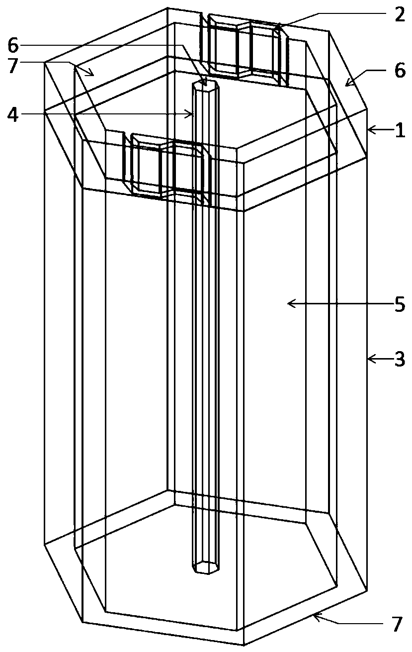
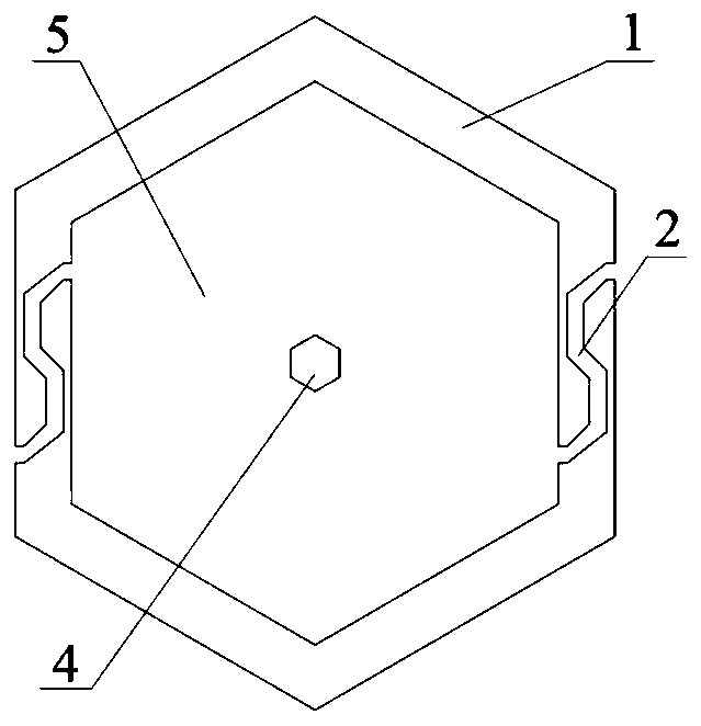
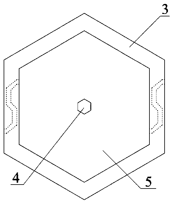
[0030] The structure of the hexagonal interlocking electrode silicon detector is as follows: Figure 1-Figure 3 As shown, it includes a hexagonal prism-shaped isolation silicon body 5, and the central axis of the isolation silicon body 5 is etched with a hexagonal prism from the top to the bottom surface, and the inner wall of the hexagonal prism is diffused and doped with boron and then filled with polysilicon to form a central electrode. 4. The six sides of the isolated silicon body 5 are etched with trenches, and the inner walls of the trenches are diffused and doped with phosphorus and filled with polysilicon to form the first trench electrode 1 and the second trench electrode 3, and isolate the silicon body 5 and the central electrode 4 , The bottom surface of the second trench electrode 3 is covered with a silicon dioxide protective layer 7, the top surface of the first trench electrode 1 and the center electrode 4 is covered with a metal contact layer 6, and the isolatio...

Embodiment 2

[0036] Modify the following dimensions of the silicon detector as follows: the height of the isolated silicon body 5 is 500 μm, the height of the first trench electrode 1 and the S-shaped isolated silicon body 2 is 50 μm, the height of the second trench electrode 3 is 450 μm, and the S-shaped The wall thickness of the isolated silicon body 2 is 4 μm, and other structures of the silicon detector are the same as those in the first embodiment.

[0037] Use the silicon detectors prepared in Examples 1 to 2 to detect incident particles. According to the test results, it can be known that enough carriers need to be excited after the incident particles enter the silicon detector, and can only be obtained when the influence of interface charges is small. Better electrical signal, if the height of the silicon detector is too small, the carriers generated by the incident particles will be easily affected by the charge on the upper and lower interfaces of the silicon detector, resulting i...

Embodiment 3

[0039] Without changing the size and position of each structure in the detection unit of Embodiment 1, only the gaps of the two C-shaped groove electrodes are set as a straight line through the center electrode 4, and the junction of the two C-shaped groove electrodes is assembled. A straight opening is left.


PUM

PropertyMeasurementUnit
heightaaaaaaaaaa
thicknessaaaaaaaaaa
thicknessaaaaaaaaaa

Abstract

The invention discloses a hexagonal interlocked electrode three-dimensional silicon detector. The detector comprises a hexagonal-prism-shaped isolation silicon body, and a central electrode is axiallyarranged in the center of the isolation silicon body; six side surfaces of the isolation silicon body are provided with first and second trench electrodes which are spliced up and down; the first trench electrode is formed by buckling two C-shaped trench electrodes, wherein metal contact layers are arranged at the tops of the first trench electrode and the central electrode, and a silicon dioxideprotective layer is arranged at the top of the isolation silicon body between the metal contact layers; and silicon dioxide protective layers are arranged at the bottoms of the second trench electrode, the central electrode and the isolation silicon body. According to the invention, the hexagonal interlocked electrode three-dimensional silicon detector prepared by the method is small in dead zone, uniform in internal electric field distribution, good in charge collection performance, good in unit independence between detection units, high in detection efficiency and high in utilization rate of silicon wafers.

Description

technical field [0001] The invention belongs to the technical field of high-energy physics and astrophysics, and relates to a three-dimensional silicon detector with hexagonal interlocking electrodes. Background technique [0002] In 1997, S.Parker et al. first proposed the first generation of silicon detectors with three-dimensional columnar electrodes. There is a high electric field area near the electrode of the detector, and a low electric field area in the center of electrode symmetry. The uneven distribution of the electric field makes the silicon detector in high radiation It is limited when used in the environment; in order to further enhance the radiation resistance of silicon detectors, in 2009, scientists from the Brookhaven National Laboratory in the United States proposed a new type of three-dimensional silicon detector, that is, a three-dimensional trench electrode silicon detector. The detection units of the columnar electrode silicon detector and the three-di...

Claims


Application Information

Patent Timeline
Patent Type & Authority Applications(China)
IPC IPC(8): H01L31/0224H01L31/08H01L31/18
CPCH01L31/0224H01L31/085H01L31/1804Y02P70/50
Inventor 李正聂谦刘曼文
Owner XIANGTAN UNIV
Why Eureka
Try Eureka