p-GaN enhanced AlGaN/GaN high-electron-mobility transistor

A high electron mobility, enhanced technology, applied in the direction of circuits, electrical components, semiconductor devices, etc., can solve the problems of threshold voltage and output current reduction, device avalanche breakdown, current collapse effect, etc., and achieve the improvement of breakdown voltage , The effect of increasing the peak value of the electric field and increasing the drop of the peak electric field

Inactive Publication Date: 2017-05-31
XIDIAN UNIV
View PDF3 Cites 10 Cited by
  • Summary
  • Abstract
  • Description
  • Claims
  • Application Information

AI Technical Summary

Problems solved by technology

[0006] In order to solve the device avalanche breakdown and current collapse effect caused by the peak electric field at the gate edge of the p-GaN enhanced AlGaN / GaN high electron mobility transistor in the prior art, the threshold voltage and output current are reduced, and the reliability is reduced etc., the present invention provides a novel p-GaN enhanced AlGaN / GaN high electron mobility transistor

Method used


Image

  • p-GaN enhanced AlGaN/GaN high-electron-mobility transistor
  • p-GaN enhanced AlGaN/GaN high-electron-mobility transistor

Examples


Embodiment Construction

[0030] In order to make the technical problems, technical solutions and advantages to be solved by the present invention clearer, a detailed description will be given below in conjunction with the accompanying drawings and specific embodiments.

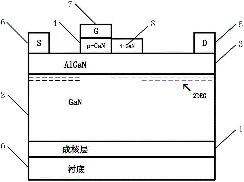
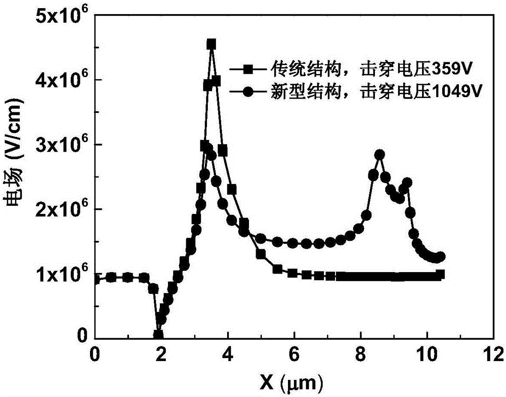
[0031] Aiming at the problem that there is a peak electric field at the gate edge of the existing p-GaN enhanced AlGaN / GaN high electron mobility transistor, the present invention provides a novel p-GaN enhanced AlGaN / GaN high electron mobility transistor with a partial intrinsic GaN cap layer. Electron mobility transistors.

[0032] Its structure is as figure 1 As shown, it mainly includes: semi-insulating substrate 0; heteroepitaxially grown AlN nucleation layer 1 on the semi-insulating substrate; GaN buffer layer 2 epitaxially grown on the AlN nucleation layer; epitaxially grown on the GaN buffer layer AlGaN barrier layer 3; p-type GaN dielectric layer 4, drain 5 and source 6 located on the AlGaN barrier layer; gate 7 located on t...


PUM


Abstract

The invention discloses a p-GaN enhanced AlGaN/GaN high-electron-mobility transistor with a partially intrinsic GaN cap layer. According to the transistor structure, the intrinsic GaN cap layer is introduced into a transistor grid electrode and the edge of a p type GaN medium layer of the transistor grid electrode, the two-dimensional electron gas concentration of a conducting channel in the area can be reduced by means of the intrinsic GaN cap layer, and the electric field modulation effect is achieved. A new electric field peak is generated, so that the high electric field of the grid edge is reduced, and an electric field on the surface of the transistor is distributed more evenly. Compared with a traditional p-GaN enhanced structure, the breakdown voltage and reliability of the novel structure are obviously improved.

Description

technical field [0001] The invention relates to the technical field of semiconductor devices, in particular to a p-GaN enhanced AlGaN / GaN high electron mobility transistor. Background technique [0002] Due to the limitations of the first-generation and second-generation semiconductor materials represented by Si and GaAs, the third-generation wide-bandgap semiconductor materials have been developed rapidly because of their excellent performance. As one of the cores of the third-generation semiconductor materials, GaN material is special in its polarization effect compared with Si, GaAs and SiC. Taking advantage of this particularity, people have developed AlGaN / GaN high electron mobility transistors, and AlGaN / GaN HEMTs are GaN-based microelectronic devices based on AlGaN / GaN heterojunction materials. The AlGaN / GaN heterojunction forms a high-density two-dimensional electron gas (two dimensional electron gas, 2DEG) at the heterojunction interface through spontaneous polariz...

Claims


Application Information

Patent Timeline
Patent Type & Authority Applications(China)
IPC IPC(8): H01L29/06H01L29/778
Inventor 段宝兴郭海君谢慎隆袁嵩杨银堂
Owner XIDIAN UNIV
Why Eureka
Try Eureka