RF ldmos device

A device and radio frequency technology, applied in the field of LDMOS field effect transistors, can solve the problems of increasing surface scattering in the drift region, reducing carrier mobility, reducing device saturation current, etc., to optimize electric field distribution, improve electric field distribution, and improve breakdown The effect of voltage

Inactive Publication Date: 2018-05-01
UNIV OF ELECTRONICS SCI & TECH OF CHINA +1
View PDF4 Cites 0 Cited by
  • Summary
  • Abstract
  • Description
  • Claims
  • Application Information

AI Technical Summary

Problems solved by technology

However, in conventional RF LDMOS, there is an electric field peak at the right edge of the Faraday cage, which makes the device prone to breakdown
In addition, a larger electric field in the drift region will increase the surface scattering in the drift region and reduce the carrier mobility, thereby reducing the saturation current of the device
The breakdown voltage of RF LDMOS has a trade-off relationship with the cut-off frequency, and the traditional Faraday shield reduces the parasitic capacitance C gd , and also introduces a high electric field near the edge of the Faraday cage near the drain, which affects the robustness of the device

Method used


Image

  • RF ldmos device
  • RF ldmos device
  • RF ldmos device

Examples


Embodiment Construction

[0025] Embodiments of the present invention are described below through specific examples, and those skilled in the art can easily understand other advantages and effects of the present invention from the content disclosed in this specification. The present invention can also be implemented or applied through other different specific implementation modes, and various modifications or changes can be made to the details in this specification based on different viewpoints and applications without departing from the spirit of the present invention.

[0026] Below in conjunction with accompanying drawing, describe technical scheme of the present invention in detail:

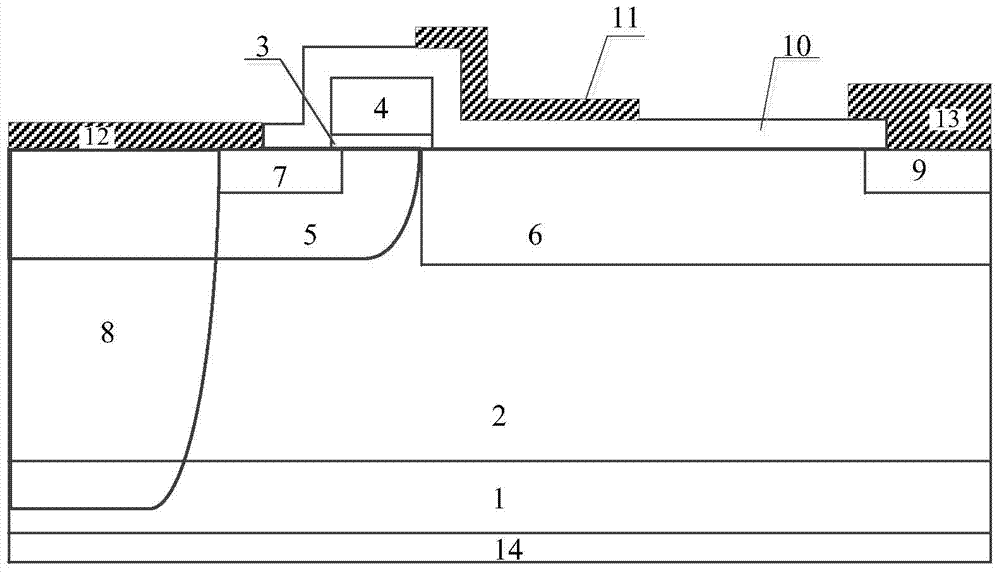
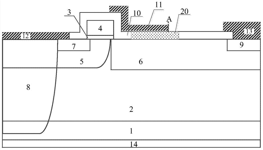
[0027] A radio frequency LDMOS device, comprising: a P+ substrate 1, a P-type epitaxial layer 2 on the P+ substrate 1, a substrate metal 14 below the P+ substrate 1, and a P+ sinker region 8 inside the P-type epitaxial layer 2, The P well 5 above the P+ sinker region 8, the N-drift region 6 on the right side of the P ...


PUM


Abstract

The present invention provides a radio frequency LDMOS device, comprising: a P+ substrate, a P-type epitaxial layer, a substrate metal, a P+sinker region inside the P-type epitaxial layer, a P well, an N-drift region, an N+ region, polysilicon, N- A Faraday cover is arranged above the drift region and on the right side of the polysilicon, and there is a layer of low k medium between the Faraday cover and the drift region, and the dielectric constant of the low k dielectric material is less than that of SiO2; the present invention is above the drift region and The insulating dielectric layer under the Faraday cover is made of low k material. This structure can effectively reduce the high electric field near the edge of the Faraday cover. Compared with the traditional structure, this device can effectively optimize the electric field distribution on the surface of the drift region, making it more uniform and improving The breakdown voltage of the device; it can also reduce the source-drain on-resistance of the device and increase the output power of the device.

Description

technical field [0001] This application relates to the field of semiconductor devices, in particular to an LDMOS field effect transistor for radio frequency applications. Background technique [0002] RF LDMOS (Laterally Double-Diffused Metal Oxide Semiconductors) field effect transistor is a high-power RF device with a wide range of applications. It has good linearity, high power gain, high withstand voltage, good matching performance, high output power and low cost. Advantages, widely used in wireless communications, mobile base stations, radar and navigation and other fields. [0003] In the application of high-power RF LDMOS devices, it is generally expected that the device has a large breakdown voltage, large output power and high frequency characteristics. In the RF LDMOS design process, in order to improve the performance of the device, the general goals pursued are: large breakdown voltage, low on-resistance, large saturation current and small parasitic capacitance ...

Claims


Application Information

Patent Timeline
Patent Type & Authority Patents(China)
IPC IPC(8): H01L29/78H01L29/06
CPCH01L29/0607H01L29/7816
Inventor 邓小川梁坤元甘志刘冬冬张波
Owner UNIV OF ELECTRONICS SCI & TECH OF CHINA
Why Eureka
Try Eureka