

Semiconductor device
a technology of semiconductor devices and semiconductor devices, applied in the direction of semiconductor devices, electrical devices, transistors, etc., can solve the problems of gcr to improve the performance of flash memory cells, and achieve the effects of improving the overlapped area, reducing the operation voltage of semiconductor devices, and improving the performance of semiconductor devices
- Summary
- Abstract
- Description
- Claims
- Application Information
AI Technical Summary
Benefits of technology
Problems solved by technology
Method used
Image

Examples
Embodiment Construction
[0016]To provide a better understanding of the present invention, preferred exemplary embodiments will be described in detail. The preferred exemplary embodiments of the present invention are illustrated in the accompanying drawings with numbered elements.
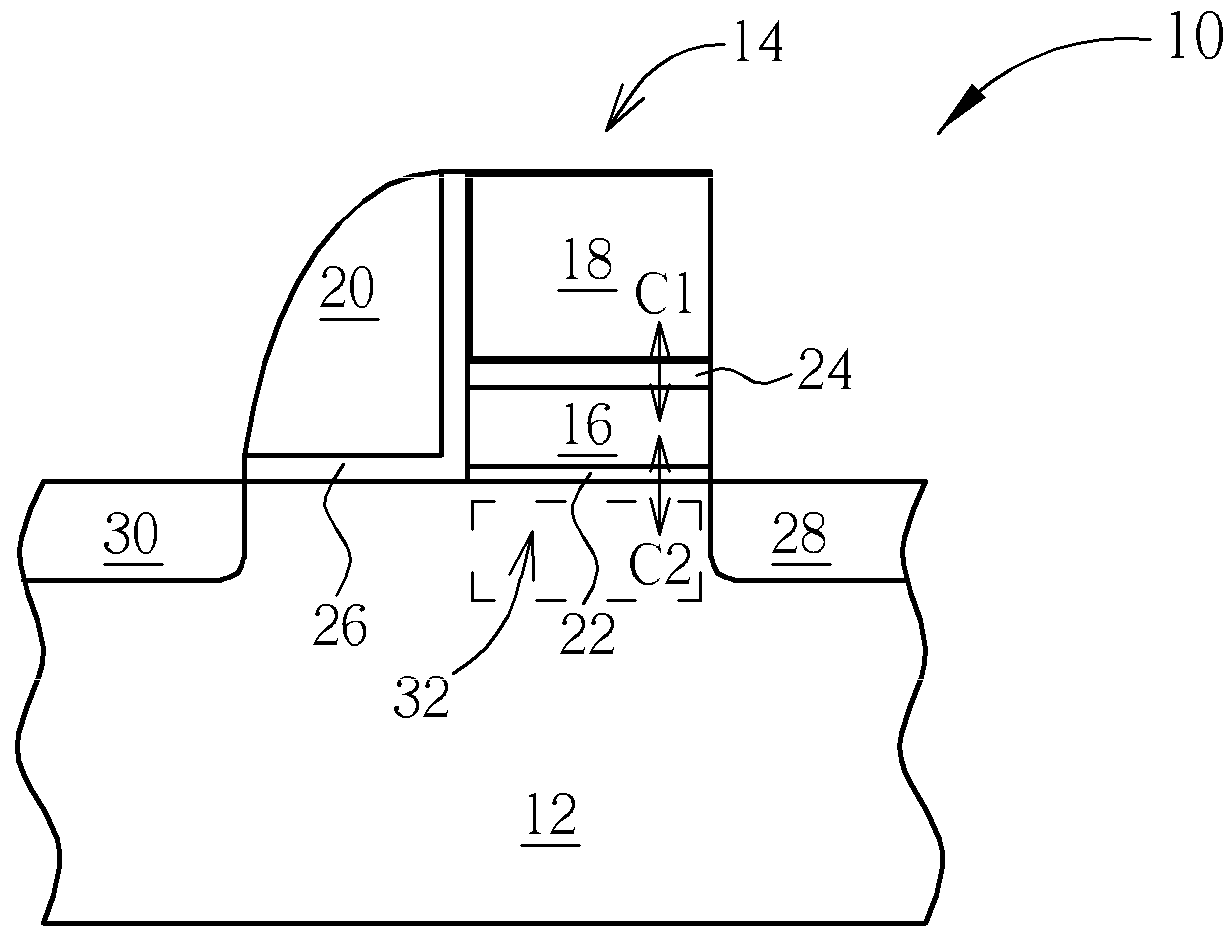
[0017]Please refer to FIG. 1, which is a cross-sectional diagram illustrating a semiconductor device according to an exemplary embodiment of the present invention. As shown in FIG. 1, a semiconductor device 10, such as a flash memory cell, includes a semiconductor substrate 12, a gate stack 14 disposed on the semiconductor substrate 12, and a select gate 20 disposed at a side of the gate stack 14. The gate stack 14 includes a floating gate 16 and a control gate 18. The semiconductor substrate 12 may include a substrate composed of Si, AsGa, silicon on insulator (SOI) layer, epitaxial layer, SiGe layer or other semiconductor materials. The floating gate 16, the control gate 18 and the select gate 20 are commonly made of polysilicon,...
PUM
 Abstract
Description
Claims
Application Information