Supercharge Your Innovation With Domain-Expert AI Agents!

Method of manufacturing semiconductor device and substrate processing apparatus

a technology of semiconductor devices and processing apparatuses, which is applied in the direction of lighting and heating apparatus, cleaning hollow objects, and liquid cleaning, etc., can solve the problems of cracks, foreign matter generation (particles), and deterioration of the yield of manufacturing semiconductor devices, so as to reduce the damage received by quartz members and increase the removal rate of sin films

Active Publication Date: 2014-11-25
KOKUSA ELECTRIC CO LTD
View PDF17 Cites 6 Cited by
  • Summary
  • Abstract
  • Description
  • Claims
  • Application Information

AI Technical Summary

Benefits of technology

[0029]According to a method of manufacturing a semiconductor device and a substrate processing apparatus of the present invention, both of the reduction of a damage received by a quartz member and the increase of a removal rate of removing the SiN film is achieved, when the inside of a processing chamber is cleaned using a cleaning gas containing fluorine elements.

Problems solved by technology

When the thin film is deposited thick, a force added thereby is increased to generate cracks and also generate foreign matters (particles) in the processing chamber in some cases.
When the foreign matters are placed on the substrate, yield of manufacturing the semiconductor device is deteriorated.

Method used


Image

  • Method of manufacturing semiconductor device and substrate processing apparatus
  • Method of manufacturing semiconductor device and substrate processing apparatus
  • Method of manufacturing semiconductor device and substrate processing apparatus

Examples


Embodiment Construction

[0040]Embodiments of the present invention will be described hereafter based on the figures.

(1) Structure of a Substrate Processing Apparatus

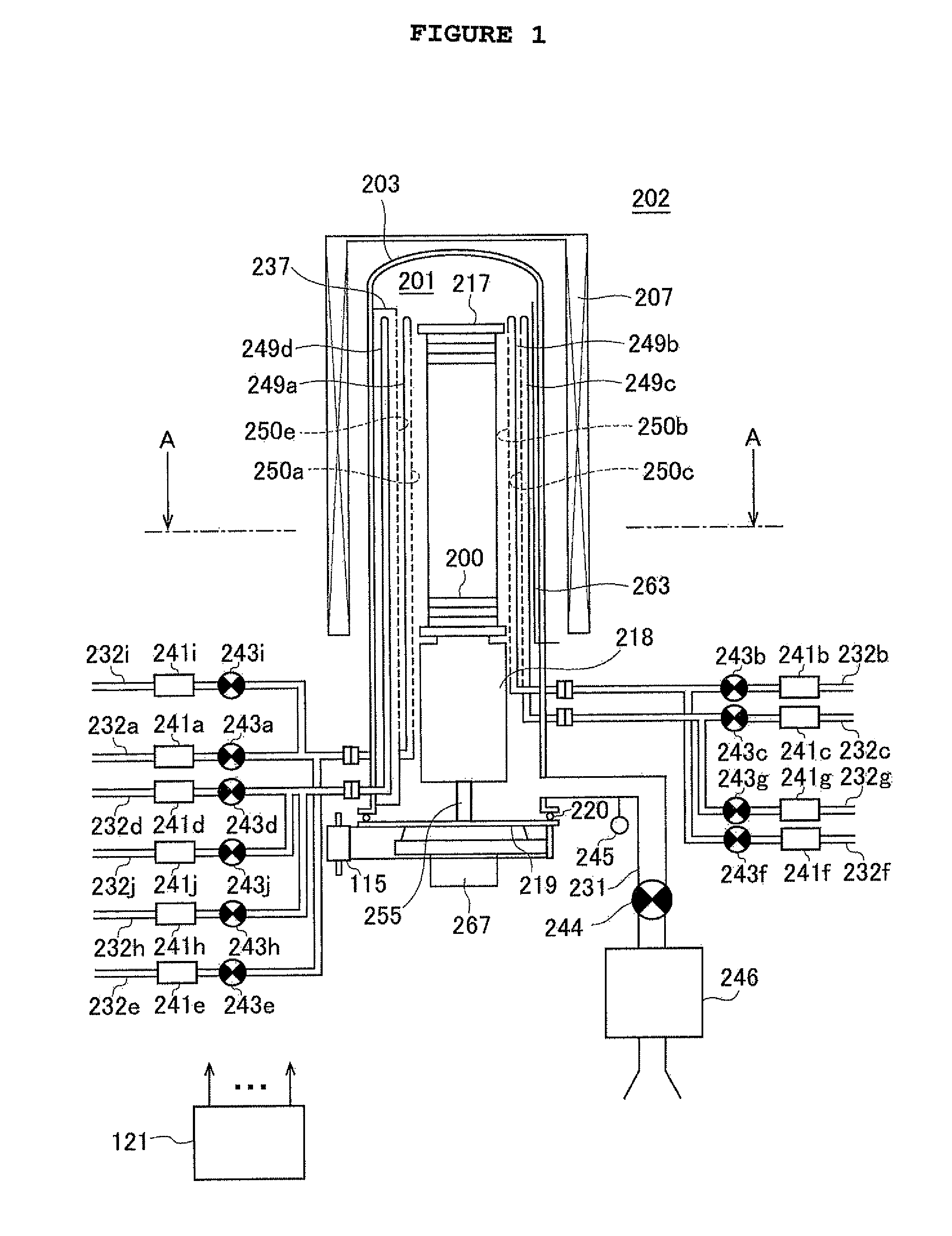
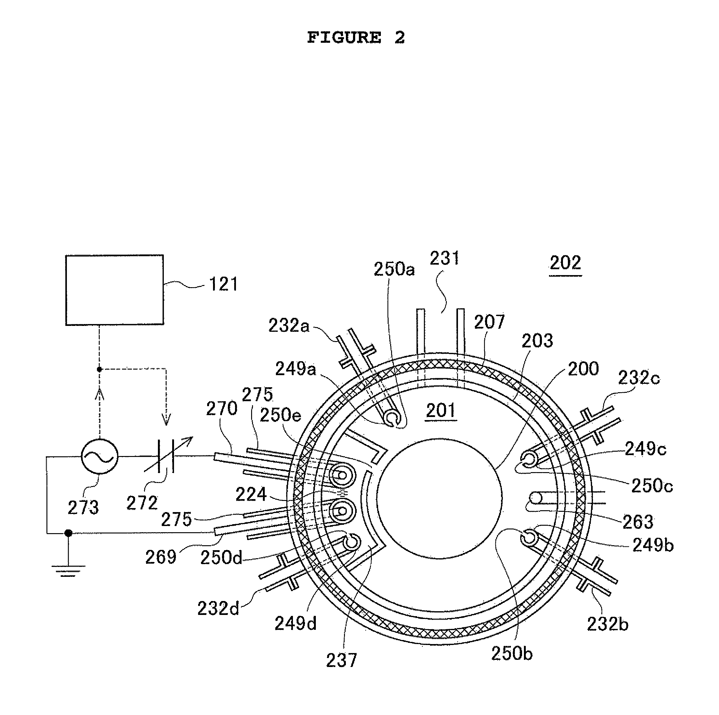
[0041]FIG. 1 is a schematic block diagram of a vertical processing furnace of a substrate processing apparatus suitably used in this embodiment, wherein a processing furnace 202 portion is shown by a vertical sectional face. FIG. 2 is a schematic block diagram of the vertical processing furnace suitably used in this embodiment, and the processing furnace 202 portion is shown by a sectional face of FIG. 1 taken along the line A-A.

[0042]As shown in FIG. 1, the processing furnace 202 has a heater 207, as a heating unit (heating mechanism). The heater 207 has a cylindrical shape, and is vertically installed by being supported by a heater base (not shown) as a holding plate. Note that the heater 207 also functions as an activation mechanism for thermally activating gas as will be described later.

[0043]A reaction tube 203 constituting a reaction vess...


PUM

PropertyMeasurementUnit
pressureaaaaaaaaaa
timeaaaaaaaaaa
temperatureaaaaaaaaaa

Abstract

To provide a method of manufacturing a semiconductor device, including: forming a thin film different from a silicon oxide film on a substrate by supplying a processing gas into a processing vessel in which the substrate is housed; removing a deposit including the thin film adhered to an inside of the processing vessel by supplying a fluorine-containing gas into the processing vessel after executing forming the thin film prescribed number of times; and forming a silicon oxide film having a prescribed film thickness on the inside of the processing vessel by alternately supplying a silicon-containing gas, and an oxygen-containing gas and a hydrogen-containing gas into the heated processing vessel in which a pressure is set to be less than an atmospheric pressure after removing the deposit.

Description

[0001]The present application is based on Japanese Patent Application No. 2010-050752, filed on Mar. 8, 2010, the entire contents of which are hereby incorporated by reference.BACKGROUND OF THE INVENTION[0002]1. Technical Field[0003]The present invention relates to a method of manufacturing a semiconductor device including forming a thin film on a substrate and a substrate processing apparatus.[0004]2. Description of the Related Art[0005]As one of the steps of manufacturing a semiconductor device, a thin film forming step can be given, which is the step of forming a thin film such as a silicon nitride film (SiN film) on a substrate. Also, the thin film forming step is the step performed by supplying a processing gas into a processing chamber into which the substrate is loaded. The thin film forming step is performed for the purpose of forming the thin film on a surface of the substrate. However, actually the thin film is formed not only on the surface of the substrate but also on an...

Claims


Application Information

Patent Timeline
Patent Type & Authority Patents(United States)
IPC IPC(8): C23C16/30B08B5/00C23C16/00C23C16/44H01L21/31C23C16/34C23C16/40H01L21/02C23C16/455
CPCC23C16/45531C23C16/347C23C16/4405C23C16/30Y10S438/905C23C16/402H01L21/0228C23C16/345H01L21/02126
Inventor AKAE, NAONORIMURAKAMI, KOTAROHIROSE, YOSHIROKAMEDA, KENJI
Owner KOKUSA ELECTRIC CO LTD
Features
  • R&D
  • Intellectual Property
  • Life Sciences
  • Materials
  • Tech Scout
  • Unparalleled Data Quality
  • Higher Quality Content
  • 60% Fewer Hallucinations
Learn More