Comparator

a comparator and comparator technology, applied in the field of comparators, can solve the problems of limiting the permitted range of input voltage vin to the comparator, mosfet with a thick gate oxide film, and difficulty in constructing a fine structure of the comparator in an integrated circuit structure, so as to avoid the breakdown of the comparator, reduce the variation range of drain voltage (or output voltage), and reduce the effect of failur

Active Publication Date: 2014-12-02
FUJI ELECTRIC CO LTD
View PDF8 Cites 5 Cited by
  • Summary
  • Abstract
  • Description
  • Claims
  • Application Information

AI Technical Summary

Benefits of technology

[0018]The present invention has been made in view of the above-described problems and an object of the present invention is to provide a comparator with a simple construction that does not breakdown a MOSFET having a thin gate oxide film and can directly compare a high input voltage.
[0025]A comparator according to the first aspect of the present invention can clamp the voltage applied between the gate and source of the differential pair of input MOSFETs by means of the Zener diodes to restrict the gate-source voltage Vgs. Consequently, the gate oxide film of the input MOSFETs is not subjected to a high voltage or high electric field strength. Therefore, the gate oxide film is reliably protected and breakdown thereof is avoided.
[0026]A comparator according to the second aspect of the invention can further limit the variation range of the drain voltage (or the output voltage) of the input MOSFET by means of negative feedback control with the feedback MOSFET. Consequently, the voltage applied between the gate and source of the input MOSFET is limited to restrict the gate-source voltage Vgs. Therefore, the gate oxide film of the input MOSFET is effectively protected together with the effect of the Zener diode.
[0027]A comparator according to the third aspect of the invention can interrupt the current from the constant current source by the semiconductor rectifying element when the source electric potential of the input MOSFET exceeds the electric potential at the current output terminal of the constant current source, thereby restricting a voltage applied between the gate and source of the input MOSFET. Therefore, the gate oxide film of the input MOSFET is more certainly protected and effectively prevented from breakdown thereof together with the protecting effects for the gate oxide film of the input MOSFET by the Zener diode and the feedback MOSFET.
[0028]Therefore, a comparator having the construction described above, even though using a MOSFET with a thin gate oxide film, can directly compare a high input voltage Vin without breakdown of the gate oxide film of the MOSFET. A comparator of the invention does not have such disadvantages as in using a thick gate oxide film and in using shunt resistors R1 and R2. In addition, the simple circuit construction of the invented comparator provides a great practical advantage.

Problems solved by technology

But the comparator has a disadvantage in that the permitted range of the input voltage Vin to the comparator is restricted by the thickness of the gate oxide film in the input MOSFETs 11 and 12 on the other hand.
A MOSFET with a thick gate oxide film, however, has difficulty in constructing a fine structure of the comparator in an integrated circuit structure.
Further problems should arise of increase in the threshold voltage of the MOSFET and decrease in the switching speed.
The use of the shunt resistors R1 and R2, however, raises new problems of not only expansion of the circuit area for the comparator in an integrated circuit structure, but also degradation of accuracy due to the scattering of the shunt resistor ratio and malfunctioning due to degradation of the SN ratio.

Method used


Image

  • Comparator
  • Comparator
  • Comparator

Examples


Embodiment Construction

[0038]The following describes in detail comparators according to some preferred embodiments of the invention with reference to accompanying drawings.

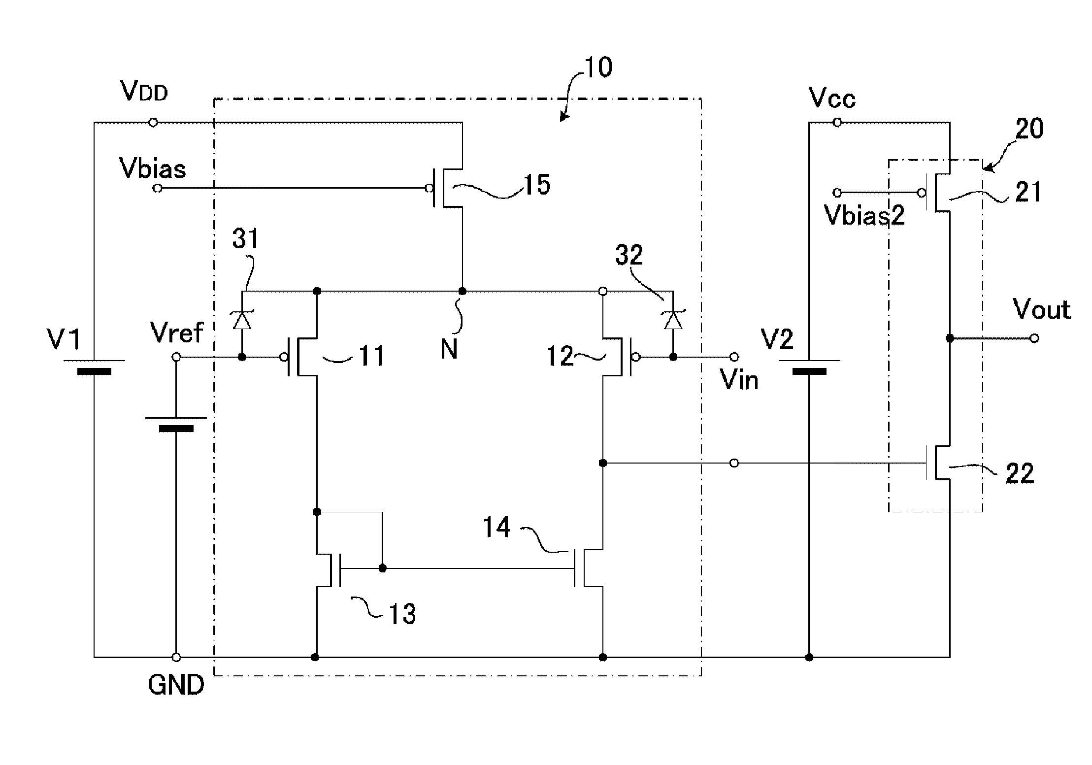
[0039]FIG. 1 shows a schematic construction of a comparator according to a first embodiment of a first aspect of the present invention. This comparator has basically a similar construction as the conventional one shown in FIG. 8, and the same components are given the same symbols. The comparator of FIG. 1 has different power supplies V1 and V2 for driving the main body comparator 10 and the inverter circuit 20, respectively.

[0040]The power supply V1 to supply a power supply voltage VDD to the main body comparator 10 is a voltage source supplying 42 V, for example. The main body comparator 10 directly compares an input voltage Vin in the range of zero to 42 V with a reference voltage Vref set at VDD / 2=21 V, for example.

[0041]The power supply V2 to supply a power supply voltage VCC to the inverter circuit 20 is a voltage source supplying ...


PUM


Abstract

A comparator comprises a differential amplifier type including input MOSFETs receiving differential input of a reference voltage and an input voltage, load MOSFETs for the input MOSFETs, and a constant current source to supply the sources of the input MOSFETs. The comparator comprises a Zener diode that is connected between the gate and source of the input MOSFETs and exhibits a breakdown voltage lower than the withstand voltage of the gate oxide film of the input MOSFET. Another comparator further comprises a feedback MOSFET that performs negative feedback of an output voltage of a main body comparator to the gates of the load MOSFETs to restrict the amplitude of the output voltage. Still another comparator further comprises a semiconductor rectifying element that exhibits a reverse-blocking characteristic higher than the power supply voltage and is interposed between the constant current source and the source of each of the input MOSFETs.

Description

CROSS-REFERENCE TO RELATED APPLICATION[0001]This application is based on, and claims priority to, Japanese Patent Application No. 2012-264808, filed on Dec. 3, 2012, contents of which are incorporated herein by reference.BACKGROUND OF THE INVENTION[0002]1. Field of the Invention[0003]The present invention relates to a comparator of a differential amplifier type with a CMOS structure, and in particular, to a comparator that performs a protection function for a gate oxide film of an input MOS-FET.[0004]2. Description of the Related Art[0005]Widely used comparators compare a reference voltage Vref and an input voltage Vin and deliver an output voltage Vout corresponding to the relative magnitude. FIG. 8 shows a schematic construction of a conventionally common comparator of a differential amplifier type having a CMOS structure. This comparator is basically composed of a main body comparator 10 of a differential amplifier type and an inverter circuit 20 that inverts the output voltage o...

Claims


Application Information

Patent Timeline
Patent Type & Authority Patents(United States)
IPC IPC(8): H03K5/22H03K5/24
CPCH03K5/2481
Inventor NAKAJIMA, HIROYUKI
Owner FUJI ELECTRIC CO LTD
Why Eureka
Try Eureka