Adjusting reference resistances in determining MRAM resistance states

a reference resistance and state technology, applied in the field of integrated circuit memories, can solve problems such as risk of reading disturb and inability to solve complete solutions, and achieve the effect of reducing the risk of changing or “disturbing” and adjusting the magnetic field in the free layer

Active Publication Date: 2014-12-02
TAIWAN SEMICON MFG CO LTD
View PDF15 Cites 14 Cited by
  • Summary
  • Abstract
  • Description
  • Claims
  • Application Information

AI Technical Summary

Benefits of technology

[0017]However, there is variability even between reference MTJ elements when two or more MTJ elements are used to produce parameter values that are used as references for one or more bit positions. An additional technique used herein to reduce the variability in the RH and RL resistances of the MTJ elements used as references, is to average resistances (or resistance-related parameter values). A plurality of reference MTJ elements in the RH state can be coupled to provide an average RH resistance; and another plurality of reference MTJ elements in the RL state can provide an average RL resistance. Alternatively, an equal number of instances of RH and RL states can be coupled in a way that derives their average resistance. The variability in the resistances of members of a population of two or more reference MTJ elements is moderated if the actual reference parameter is based on an average rather than the parameter value characteristic of one MTJ element alone.
[0022]The write current needed to assume a given RH or RL state requires a given write current polarity at least at a minimum amplitude. Reading the value of a bit, namely detecting its resistance state, also involves passing a current through the MTJ element, but the polarity is unimportant except that if the read current is applied at the polarity that might cause the present RH or RL state of the MTJ element to change, the read current bias needs to be kept at a lower current amplitude than the minimum write current amplitude, so as to reduce the risk of changing or “disturbing” the logical value stored at the bit cell. A read disturb risk can arise in situations where there is a particular combination of present resistance state and read current bias polarity. Changing an MTJ element from its high resistance state to its low resistance state requires a write current polarity that is opposite from the polarity needed when writing from a low resistance state to a high resistance state.
[0023]The present resistance state RH or RL of bit cell MTJ elements is unknown because the logic values of the cells (the stored data values) are arbitrary. Any given cell might be found in a high or low resistance state. However, by taking appropriate care with the read bias current polarity applied to reference MTJ elements in a reference circuit, it may be possible to protect the reference MTJ elements from read disturb risk.

Problems solved by technology

The variations in resistance and in the span between RH and RL present challenges in the selection of a threshold value to use for comparison when distinguishing whether an MTJ being read is in its high or low resistance state.
Using reference MTJ elements to define the basis of comparison when reading the bit cell MTJ elements is helpful but not a complete solution.
However, there is variability even between reference MTJ elements when two or more MTJ elements are used to produce parameter values that are used as references for one or more bit positions.
A read disturb risk can arise in situations where there is a particular combination of present resistance state and read current bias polarity.

Method used


Image

  • Adjusting reference resistances in determining MRAM resistance states
  • Adjusting reference resistances in determining MRAM resistance states
  • Adjusting reference resistances in determining MRAM resistance states

Examples


Embodiment Construction

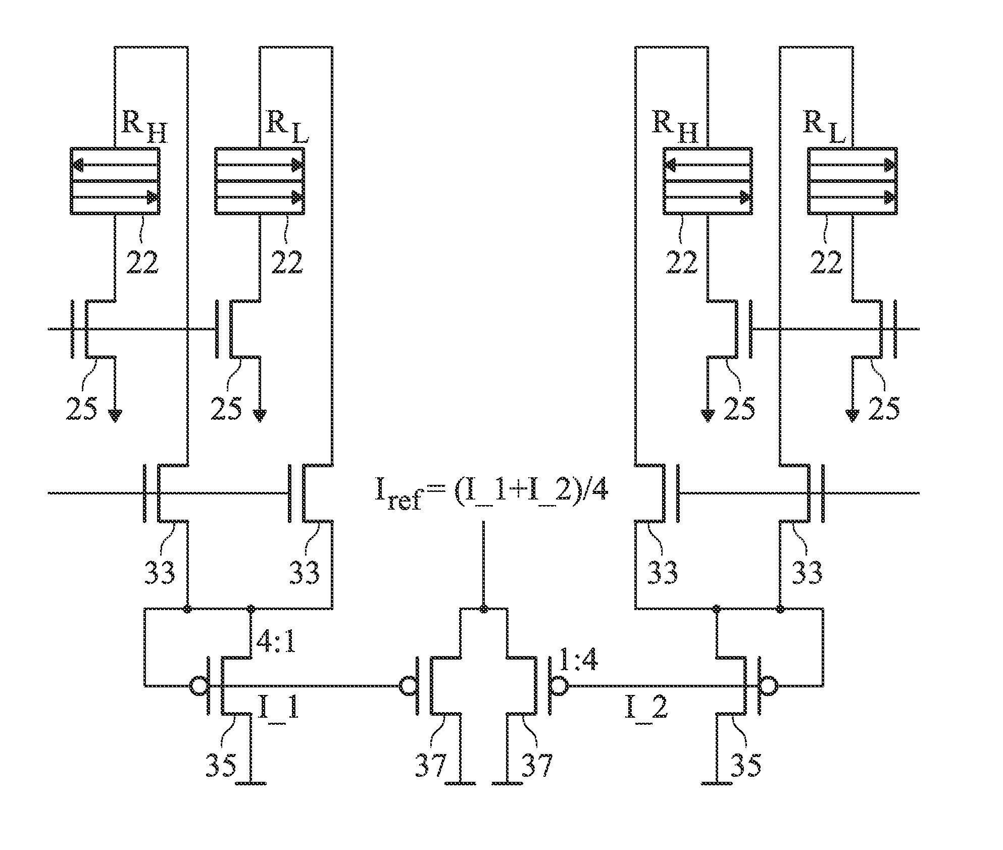
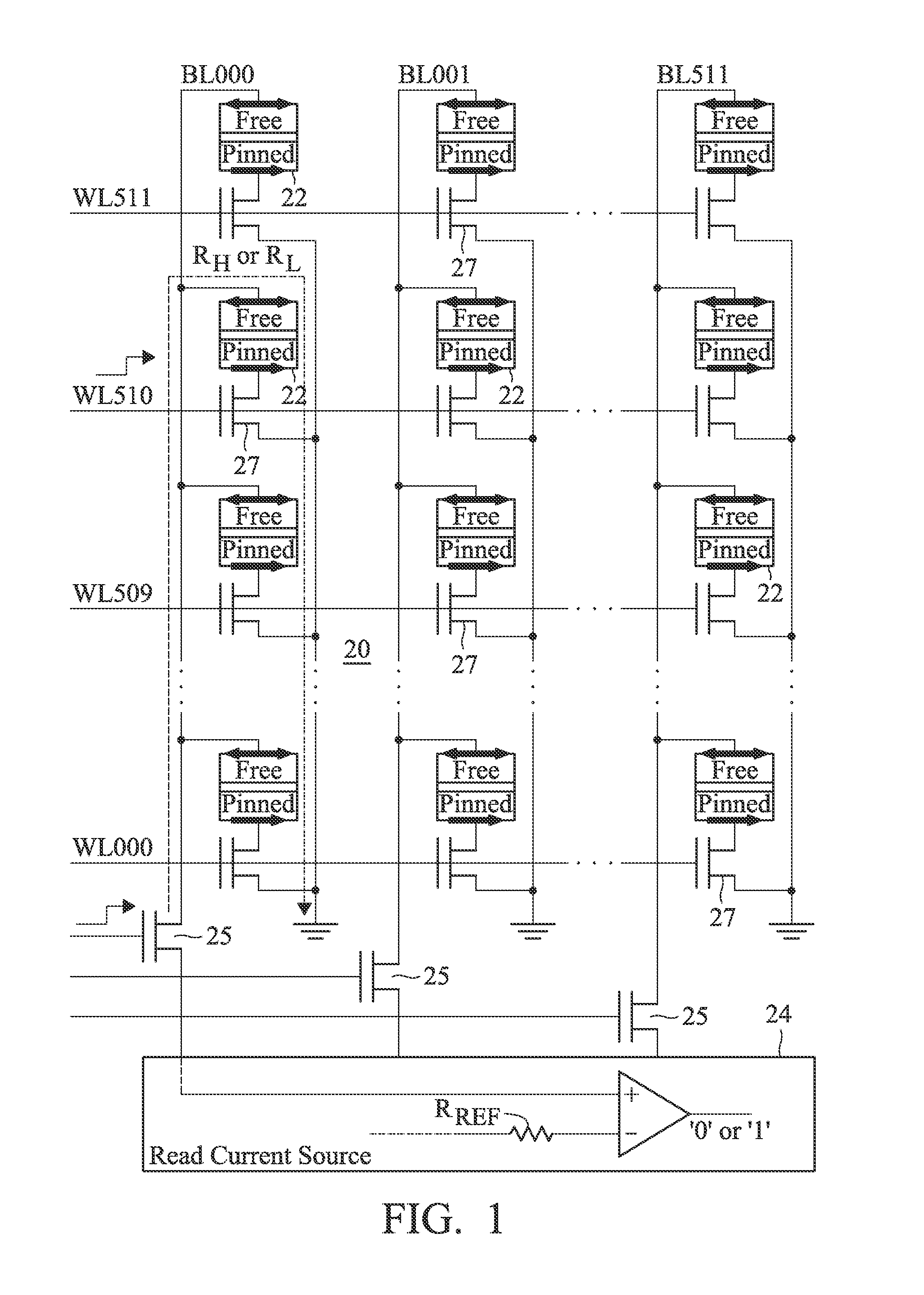
[0042]A memory bit cell using magnetoresistive techniques as provided herein uses at least one magnetic tunnel junction (MTJ) element for each bit cell. Each MTJ element comprises two superimposed magnetic layers separated by a nonmagnetic barrier layer. One of the magnetic layers has a permanent magnetic field aligned in a given direction (the pinned layer) and the other magnetic layer has a changeable magnetic field alignment (the free layer).

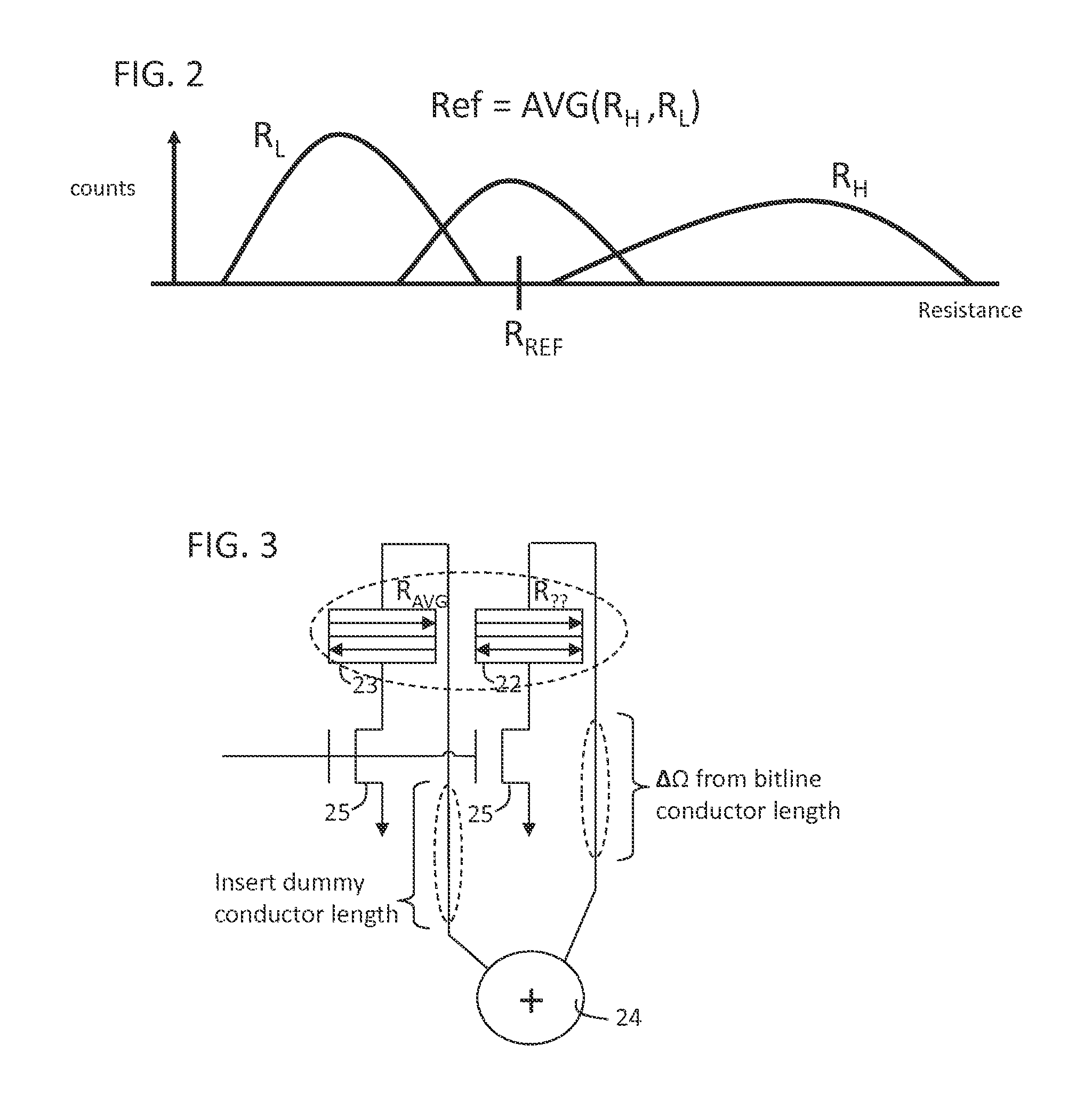
[0043]The electrical resistance of the superimposed layers (namely the series resistance through the pinned, barrier and free layers) is different when the magnetic fields of the free and pinned layers are aligned with one another (parallel) versus when the magnetic fields of the free and pinned layers are opposite (anti-parallel). The MTJ element is in a low resistance state RL when the magnetic field alignments are parallel, or in a high resistance state RH when the magnetic field orientations of the two layers are anti-parallel.

[0044]The m...


PUM


Abstract

Magneto-resistive memory bit cells in an array have high or low resistance states storing logic values. During read operations, a bias source is coupled to an addressed memory word, coupling a parameter related to cell resistance to a sense amplifier at each bit position. The sense amplifiers determine whether the parameter value is greater or less than a reference value between the high and low resistance states. The reference value is derived by averaging or splitting a difference of resistances of reference cells at high and / or low resistance states. Bias current is conducted over address lines with varying resistance, due to different distances between the sense amplifiers and addressed memory words, which is canceled by inserting into the comparison circuit a resistance from a dummy addressing array, equal to the resistance of the conductor addressing the selected word line and bit position.

Description

BACKGROUND[0001]This disclosure relates to integrated circuit memories wherein distinct binary logic values are represented by changeable high electrical resistance and low electrical resistance states of magneto-resistive memory elements contained in bit cells. During memory read operations, the different resistance states are distinguished using sense amplifiers that are switchably coupled to addressed bit cells. A sense amplifier compares a resistance-related parameter of an addressed bit cell, such as current amplitude at a given bias voltage, versus a related parameter in a reference circuit comprising reference magneto-resistive elements that produce a threshold level for comparison with the bit cell.[0002]This disclosure provides for reducing the effects of differences in resistance among reference elements using certain averaging techniques, and also offsets the variation in the resistance of the conductors of different lengths, that switchably couple addressed bit cells to ...

Claims


Application Information

Patent Timeline
Patent Type & Authority Patents(United States)
IPC IPC(8): G11C11/15G11C11/16
CPCG11C11/1673G11C11/16G11C11/15
Inventor CHIH, YUE-DERHUANG, CHIN-YILIN, CHUN-JUNGLIN, KAI-CHUNYU, HUNG-CHANG
Owner TAIWAN SEMICON MFG CO LTD
Why Eureka
Try Eureka